Friday, August 13th 2021

AMD Ryzen 5 5600G APU Die Shots Published
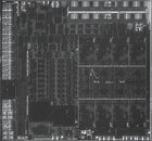
We have recently seen the first high-resolution die shots of AMD's Ryzen 5 5600G Cezanne APU thanks to the work of Fritzchens Fritz. The photos show the internal layout of the processor with its Zen 3 CPU, Vega GPU, and corresponding components. To get these shots, the chip had to be delidded by removing the IHS which has been made harder with the move to a soldered design. The Ryzen 5 5600G is a 6 core, 12 thread part with 7 Vega GPU cores which can all be seen in the annotated diagram of the die created by Locuza. The diagram also shows the suspected locations of various PCIe 3.0, and memory controllers along with cache placements for the CPU and GPU. The processor is manufactured on TSMC's 7 nm process and features a total of 10.7 Billion transistors packed into the 180 mm² die.
Sources:
Fritzchens Fritz, @Locuza_


31 Comments on AMD Ryzen 5 5600G APU Die Shots Published
AMD could triple the performance of their IGP and there'd still be no overlap with their dGPUs.
HEDT CPU with very high power delivery (400-500W) in STRX4 socket. only 16 CPU cores but full RDNA2 (or newer) die and 16GB HBM.
Only high end watercooling need apply.
The gamer IGP is what will be build into the Steam Deck. This here was always planned as a fast CPU for work which can put out an 2D image without an dedicated GPU. And for that the GPU part is still too big while lacking fixed function decoding for AV1 and high resolution output via HDMI 2.1.