Wednesday, March 19th 2025

NVIDIA Unveils Vera CPU and Rubin Ultra AI GPU, Announces Feynman Architecture

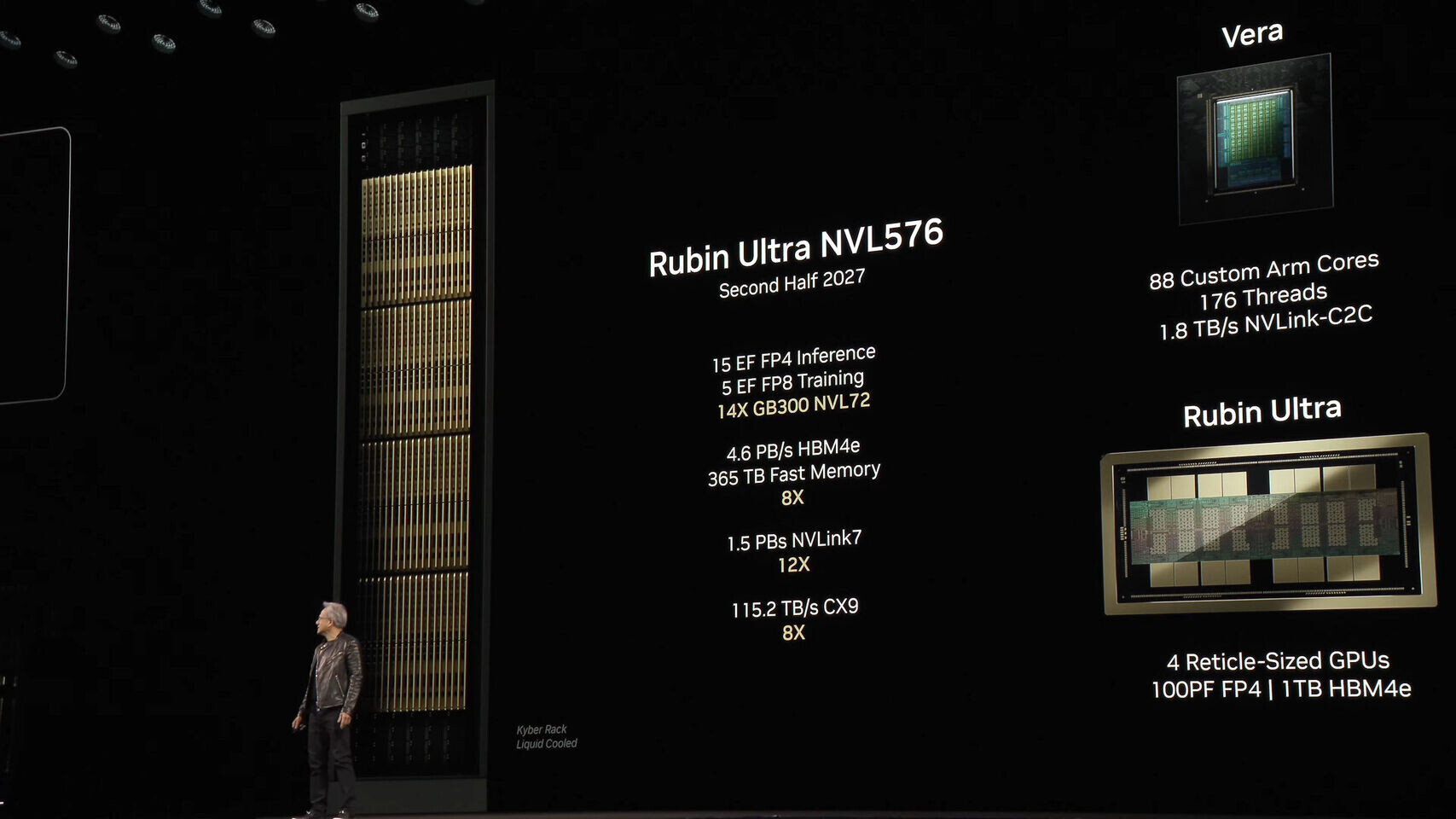
NVIDIA at GTC 2025 announced its next-generation flagship AI GPU, the Rubin Ultra. A successor to the Blackwell Ultra unveiled this year, Rubin Ultra is slated for the second half of 2027. A single Rubin Ultra package contains four AI GPU dies joined at the hip with die-to-die bonding and a fast interconnect that enables cache coherency. The package also features a whopping 1 TB of HBM4e memory. NVIDIA is claiming a performance target of 100 petaFLOPs FP4 per package.

The company also unveiled its next-generation CPU for AI supercomputers, called simply the Vera CPU. A successor to Grace, Vera comes with 88 Arm CPU cores. These are custom high-performance cores designed by NVIDIA, and aren't carried over from the reference Arm Cortex family. The cores support SMT, giving the CPU 176 logical processors. The chip comes with a 1.8 TB/s NVLink C2C connection. Lastly, the company announced that the architecture succeeding Rubin will be codenamed Feynman, after Richard Feynman. The company is looking to debut the first silicon based on Feynman in 2028.
Source: VideoCardz
Add your own comment

13 Comments on NVIDIA Unveils Vera CPU and Rubin Ultra AI GPU, Announces Feynman Architecture

#1
Athena
I wonder how many 0's they will add to the price of this...
Posted on Reply
#2
N/A
Rubin GDDR7 when.
Posted on Reply
#3
Tomorrow
N/ARubin GDDR7 when.
Wont be. Rubin will likely be more like Volta.
Feynman in 2028 seems to be the RTX 6000 series.

At least that's what im reading from this news. Next year they will likely release Blackwell based Super series. Possibly with 3GB G7 modules. Maybe based on Blackwell Ultra.
Posted on Reply
#4
ncrs
TomorrowWont be. Rubin will likely be more like Volta.
Feynman in 2028 seems to be the RTX 6000 series.

At least that's what im reading from this news. Next year they will likely release Blackwell based Super series. Possibly with 3GB G7 modules. Maybe based on Blackwell Ultra.
Blackwell the datacenter design (B100/B200/GB200) and Blackwell 2.0 the consumer design (GB202/GB203/GB205...) are already split. They share common underlying architecture, but are not the same. It would make sense to repeat the same split for Rubin and subsequent iterations.
It's unlikely that Blackwell Ultra (B300/GB300) will be made a consumer design in its raw form. I haven't seen any details about what changed between B100 and B300 so we don't know if those changes already made it to consumer GB202 for example.
Posted on Reply
#5
Tomorrow
ncrsBlackwell the datacenter design (B100/B200/GB200) and Blackwell 2.0 the consumer design (GB202/GB203/GB205...) are already split. They share common underlying architecture, but are not the same. It would make sense to repeat the same split for Rubin and subsequent iterations.
It's unlikely that Blackwell Ultra (B300/GB300) will be made a consumer design in its raw form. I haven't seen any details about what changed between B100 and B300 so we don't know if those changes already made it to consumer GB202 for example.
Consumer cards follow two year cadence. Since Blackwell 2.0 as you call it was released at the beginning of 2025, then it is logical to assume that the next consumer architecture wont launch before 2027. At the beginning of 2027 it could be Rubin yes, but i doubt it. Rubin Ultra is end of 2027 so that's doubtful and Feynman is 2028.

When it comes to Super refresh it depends. If Nvidia is content with just a memory capacity upgrade (assuming we even get it) then yes it will be the same Blackwell we have now. If they also plan on increasing performance then it would make sense to use Blackwell Ultra for 2026.
Posted on Reply
#6
igormp
ncrsIt's unlikely that Blackwell Ultra (B300/GB300) will be made a consumer design in its raw form. I haven't seen any details about what changed between B100 and B300 so we don't know if those changes already made it to consumer GB202 for example.
TomorrowIf they also plan on increasing performance then it would make sense to use Blackwell Ultra for 2026.
AFAIK the Ultra variant has no chances to the main GPU die architecture, they upgraded the memory subsystem with denser stacks to reach 288GB (compared to the previous 192GB and the networking stack (CX8 instead of CX7). Raw perf is still the same between the B200 and B300.

Rub Ultra is likely a similar scheme, exact same architecture, but with double the amount of chips in a bigger package, with denser (maybe faster?) memory.

A super variant on the consumer space may either use just 3GB modules, or actually do that and use some faster modules. Current product stack uses 28Gbps modules, but AFAIK there are 30Gbps+ modules already out there, doesn't the 5080 already makes use of one of those faster variants?
So yeah, bump memory capacity, make memory faster, and keep the prices the same or even give it some discount, in a similar fashion to what we saw with the 4080 Super.
Posted on Reply
#7
Tomorrow
I think SK Hynix showed 40Gbps G7. That's reasonably faster than today's 28-30Gbps. Especially considering G6X to G7 was at worst only 23Gbps (4080S) to 28Gbps jump.
Posted on Reply
#8
ncrs
TomorrowConsumer cards follow two year cadence. Since Blackwell 2.0 as you call it was released at the beginning of 2025, then it is logical to assume that the next consumer architecture wont launch before 2027. At the beginning of 2027 it could be Rubin yes, but i doubt it. Rubin Ultra is end of 2027 so that's doubtful and Feynman is 2028.

When it comes to Super refresh it depends. If Nvidia is content with just a memory capacity upgrade (assuming we even get it) then yes it will be the same Blackwell we have now. If they also plan on increasing performance then it would make sense to use Blackwell Ultra for 2026.
Rubin is scheduled for second half of 2026 (source: STH), so the timing fits.
igormpAFAIK the Ultra variant has no chances to the main GPU die architecture, they upgraded the memory subsystem with denser stacks to reach 288GB (compared to the previous 192GB and the networking stack (CX8 instead of CX7). Raw perf is still the same between the B200 and B300.
Blackwell Ultra is to have new instructions vs. GB200 (source: STH), so it's not just a simple memory subsystem upgrade. The slide also shows increased performance of B300 - 15 petaflop Dense FP4 vs. B200's 10 petaflop.
Posted on Reply
#9
igormp
ncrsBlackwell Ultra is to have new instructions vs. GB200 (source: STH), so it's not just a simple memory subsystem upgrade. The slide also shows increased performance of B300 - 15 petaflop Dense FP4 vs. B200's 10 petaflop.
That comparison was to Hopper, not the GB200. Here are the specs for both:


www.nvidia.com/en-us/data-center/gb200-nvl72/?ncid=no-ncid
www.nvidia.com/en-us/data-center/gb300-nvl72/

As you can see, the raw perf numbers are pretty much the same. The major difference is the increased VRAM.
I also just noticed that the CPU is now using SOCAMM, interesting.
Posted on Reply
#10
ncrs
igormpThat comparison was to Hopper, not the GB200. Here are the specs for both:
If so then why does the slide specifically say "1.5X GB200 NVL72"? I think this increased performance is for those two specific metrics. The specification you linked only shows sparse FP4 for GB200, and is preliminary for Blackwell Ultra. Tom's Hardware has more specs in their article, but again without much official confirmation.
igormpAs you can see, the raw perf numbers are pretty much the same. The major difference is the increased VRAM.
I also just noticed that the CPU is now using SOCAMM, interesting.
I'm not so sure they would make such a big deal out of Blackwell Ultra if performance stayed exactly the same. Anyway we'll see when NVIDIA releases more docs.
Posted on Reply
#11
igormp
ncrsIf so then why does the slide specifically say "1.5X GB200 NVL72"?
Have you seen the actual conference? Those 1.5X GB200 are referring to the memory. The rest is referring to Hopper. Misleading graphs, as always.
ncrsThe specification you linked only shows sparse FP4 for GB200, and is preliminary for Blackwell Ultra. Tom's Hardware has more specs in their article, but again without much official confirmation.
Their DGX GB300 shows pretty similar numbers to the one I gave you before:

www.nvidia.com/en-us/data-center/dgx-gb300/

Anyhow, the ratio between FP32:FP16:FP8/INT8:FP4/INT4 is always 1:2:4:8. 360 PFlop FP8 sparse perf from the slides presented still match the numbers from GB200, so no difference in this regard.
It wouldn't make any sense for the perf ratio between data types to change.
ncrsI'm not so sure they would make such a big deal out of Blackwell Ultra if performance stayed exactly the same. Anyway we'll see when NVIDIA releases more docs.
More memory and better networking is EXTREMELY relevant for larger models. GPU clusters often stay at 20~40% utilization due to the communication bottleneck. More memory means you can fit bigger models at the same number of nodes, or use way less nodes for the same model (which implies in less communication overhead).
It's the exact same thing between the H100 and H200, just a memory subsystem upgrade (although the H200 got both more memory AND extra memory bandwidth).
Posted on Reply
#12
ncrs
igormpHave you seen the actual conference? Those 1.5X GB200 are referring to the memory. The rest is referring to Hopper. Misleading graphs, as always.
I've read the STH coverage of it since I can't stand long periods of Mr. Huang ;)
It seems that the slides were indeed misleading as the DGX specs don't have the preliminary indicator and match your argument. Thanks for linking it.
Posted on Reply
#13
igormp
ncrsI can't stand long periods of Mr. Huang
What do you mean you don't like to see that glorious leather jacket, which now even has path tracing? :laugh:
Posted on Reply
Add your own comment
Mar 23rd, 2025 09:14 EDT change timezone

New Forum Posts

Popular Reviews

Controversial News Posts