News Posts matching #Rubin

Return to Keyword Browsing

Next‑Gen HBM4 to HBM8: Toward Multi‑Terabyte Memory on 15,000 W Accelerators

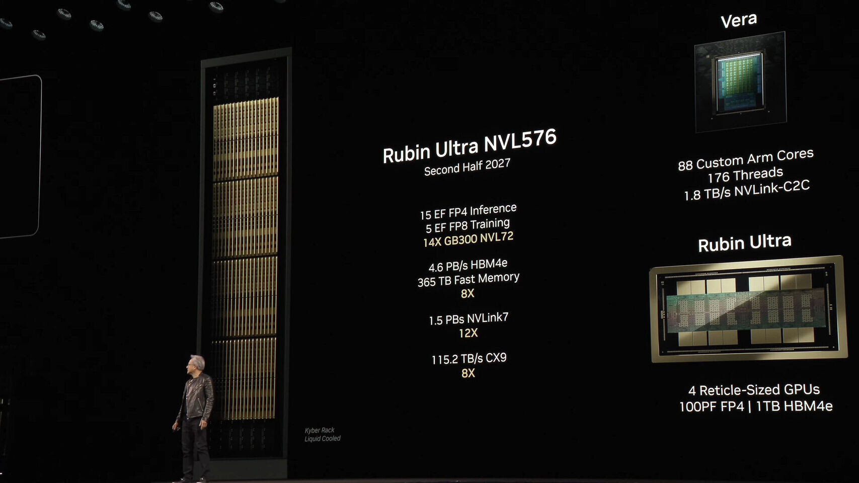
In a joint briefing this week, KAIST's Memory Systems Laboratory and TERA's Interconnection and Packaging group presented a forward-looking roadmap for High Bandwidth Memory (HBM) standards and the accelerator platforms that will employ them. Shared via Wccftech and VideoCardz, the outline covers five successive generations, from HBM4 to HBM8, each promising substantial gains in capacity, bandwidth, and packaging sophistication. First up is HBM4, targeted for a 2026 rollout in AI GPUs and data center accelerators. It will deliver approximately 2 TB/s per stack at an 8 Gbps pin rate over a 2,048-bit interface. Die stacks will reach 12 to 16 layers, yielding 36-48 GB per package with a 75 W power envelope. NVIDIA's upcoming Rubin series and AMD's Instinct MI500 cards are slated to employ HBM4, with Rubin Ultra doubling the number of memory stacks from eight to sixteen and AMD targeting up to 432 GB per device.

Looking to 2029, HBM5 maintains an 8 Gbps speed but doubles the I/O lanes to 4,096 bits, boosting throughput to 4 TB/s per stack. Power rises to 100 W and capacity scales to 80 GB using 16‑high stacks of 40 Gb dies. NVIDIA's tentative Feynman accelerator is expected to be the first HBM5 adopter, packing 400-500 GB of memory into a multi-die package and drawing more than 4,400 W of total power. By 2032, HBM6 will double pin speeds to 16 Gbps and increase bandwidth to 8 TB/s over 4,096 lanes. Stack heights can grow to 20 layers, supporting up to 120 GB per stack at 120 W. Immersion cooling and bumpless copper-copper bonding will become the norm. The roadmap then predicts HBM7 in 2035, which includes 24 Gbps speeds, 8,192-bit interfaces, 24 TB/s throughput, and up to 192 GB per stack at 160 W. NVIDIA is preparing a 15,360 W accelerator to accommodate this monstrous memory.

Micron Ships HBM4 Samples: 12-Hi 36 GB Modules with 2 TB/s Bandwidth

Micron has achieved a significant advancement of the HBM4 architecture, which will stack 12 DRAM dies (12-Hi) to provide 36 GB of capacity per package. According to company representatives, initial engineering samples are scheduled to ship to key partners in the coming weeks, paving the way for full production in early 2026. The HBM4 design relies on Micron's established 1β ("one-beta") process node for DRAM tiles, in production since 2022, while it prepares to introduce EUV-enabled 1γ ("one-gamma") later this year for DDR5. By increasing the interface width from 1,024 to 2,048 bits per stack, each HBM4 chip can achieve a sustained memory bandwidth of 2 TB/s, representing a 20% efficiency improvement over the existing HBM3E standard.

NVIDIA and AMD are expected to be early adopters of Micron's HBM4. NVIDIA plans to integrate these memory modules into its upcoming Rubin-Vera AI accelerators in the second half of 2026. AMD is anticipated to incorporate HBM4 into its next-generation Instinct MI400 series, with further information to be revealed at the company's Advancing AI 2025 conference. The increased capacity and bandwidth of HBM4 will address growing demands in generative AI, high-performance computing, and other data-intensive applications. Larger stack heights and expanded interface widths enable more efficient data movement, a critical factor in multi-chip configurations and memory-coherent interconnects. As Micron begins mass production of HBM4, major obstacles to overcome will be thermal performance and real-world benchmarks, which will determine how effectively this new memory standard can support the most demanding AI workloads.
Micron HBM4 Memory

NVIDIA and HPE Join Forces to Construct Advanced Supercomputer in Germany

NVIDIA and Hewlett Packard Enterprise announced Tuesday at a supercomputing conference in Hamburg their partnership with Germany's Leibniz Supercomputing Centre to build a new supercomputer called Blue Lion which will deliver approximately 30 times more computing power than the current SuperMUC-NG system. The Blue Lion supercomputer will run on NVIDIA's upcoming Vera Rubin architecture. This setup combines the Rubin GPU with NVIDIA's first custom CPU Vera. The integrated system aims to unite simulation, data processing, and AI into one high-bandwidth low-latency platform. Optimized to support scientific research it boasts shared memory coherent compute abilities, and in-network acceleration.

HPE will build the system using its next-gen Cray technology by including NVIDIA GPUs along with cutting-edge storage and interconnect systems. The Blue Lion supercomputer will use HPE's 100% fanless direct liquid-cooling setup. This design circulates warm water through pipes for efficient cooling while the generated system's heat output will be reused to warm buildings nearby. The Blue Lion project comes after NVIDIA said Lawrence Berkeley National Lab in the US will also set up a Vera Rubin-powered system called Doudna next year. Scientists will have access to the Blue Lion supercomputer beginning in early 2027. The Blue Lion supercomputer, based in Germany will be utilized by researchers working on climate, physics, and machine learning. In contrast, Doudna, the U.S. Department of Energy's next supercomputer, will get its data from telescopes, genome sequencers, and fusion experiments.

Doudna Supercomputer Will be Powered by NVIDIA's Next-gen Vera Rubin Platform

Ready for a front-row seat to the next scientific revolution? That's the idea behind Doudna—a groundbreaking supercomputer announced today at Lawrence Berkeley National Laboratory in Berkeley, California. The system represents a major national investment in advancing U.S. high-performance computing (HPC) leadership, ensuring U.S. researchers have access to cutting-edge tools to address global challenges. "It will advance scientific discovery from chemistry to physics to biology and all powered by—unleashing this power—of artificial intelligence," U.S. Energy Secretary Chris Wright (pictured above) said at today's event.

Also known as NERSC-10, Doudna is named for Nobel laureate and CRISPR pioneer Jennifer Doudna. The next-generation system announced today is designed not just for speed but for impact. Powered by Dell Technologies infrastructure with the NVIDIA Vera Rubin architecture, and set to launch in 2026, Doudna is tailored for real-time discovery across the U.S. Department of Energy's most urgent scientific missions. It's poised to catapult American researchers to the forefront of critical scientific breakthroughs, fostering innovation and securing the nation's competitive edge in key technological fields.

TSMC Outlines Roadmap for Wafer-Scale Packaging and Bigger AI Packages

At this year's Technology Symposium, TSMC unveiled an engaging multi-year roadmap for its packaging technologies. TSMC's strategy splits into two main categories: Advanced Packaging and System-on-Wafer. Back in 2016, CoWoS-S debuted with four HBM stacks paired to N16 compute dies on a 1.5× reticle-limited interposer, which was an impressive feat at the time. Fast forward to 2025, and CoWoS-S now routinely supports eight HBM chips alongside N5 and N4 compute tiles within a 3.3× reticle budget. Its successor, CoWoS-R, increases interconnect bandwidth and brings N3-node compatibility without changing that reticle constraint. Looking toward 2027, TSMC will launch CoWoS-L. First up are large N3-node chiplets, followed by N2-node tiles, multiple I/O dies, and up to a dozen HBM3E or HBM4 stacks—all housed within a 5.5× reticle ceiling. It's hard to believe that eight HBM stacks once sounded ambitious—now they're just the starting point for next-gen AI accelerators inspired by AMD's Instinct MI450X and NVIDIA's Vera Rubin.

Integrated Fan-Out, or InFO, adds another dimension with flexible 3D assemblies. The original InFO bridge is already powering AMD's Instinct cards. Later this year, InFO-POP (package-on-package) and InFO-2.5D arrive, promising even denser chip stacking and unlocking new scaling potential on a single package, away from the 2D and 2.5D packaging we were used to, going into the third dimension. On the wafer scale, TSMC's System-on-Wafer lineup—SoW-P and SoW-X—has grown from specialized AI engines into a comprehensive roadmap mirroring logic-node progress. This year marks the first SoIC stacks from N3 to N4, with each tile up to 830 mm² and no hard limit on top-die size. That trajectory points to massive, ultra-dense packages, which is exactly what HPC and AI data centers will demand in the coming years.

NVIDIA Unveils Vera CPU and Rubin Ultra AI GPU, Announces Feynman Architecture

NVIDIA at GTC 2025 announced its next-generation flagship AI GPU, the Rubin Ultra. A successor to the Blackwell Ultra unveiled this year, Rubin Ultra is slated for the second half of 2027. A single Rubin Ultra package contains four AI GPU dies joined at the hip with die-to-die bonding and a fast interconnect that enables cache coherency. The package also features a whopping 1 TB of HBM4e memory. NVIDIA is claiming a performance target of 100 petaFLOPs FP4 per package.

The company also unveiled its next-generation CPU for AI supercomputers, called simply the Vera CPU. A successor to Grace, Vera comes with 88 Arm CPU cores. These are custom high-performance cores designed by NVIDIA, and aren't carried over from the reference Arm Cortex family. The cores support SMT, giving the CPU 176 logical processors. The chip comes with a 1.8 TB/s NVLink C2C connection. Lastly, the company announced that the architecture succeeding Rubin will be codenamed Feynman, after Richard Feynman. The company is looking to debut the first silicon based on Feynman in 2028.

NVIDIA Confirms: "Blackwell Ultra" Coming This Year, "Vera Rubin" in 2026

During its latest FY2024 earnings call, NVIDIA's CEO Jensen Huang gave a few predictions about future products. The upcoming Blackwell B300 series, codenamed "Blackwell Ultra," is scheduled for release in the second half of 2025. It will feature significant performance enhancements over the B200 series. These GPUs will incorporate eight stacks of 12-Hi HBM3E memory, providing up to 288 GB of onboard memory, paired with the Mellanox Spectrum Ultra X800 Ethernet switch, which offers 512 ports. Earlier rumors suggested that this is a 1,400 W TBP chip, meaing that NVIDIA is packing a lot of compute in there. There is a potential 50% performance increase compared to current-generation products. However, NVIDIA has not officially confirmed these figures, but rough estimates of core count and memory bandwidth increase can make it happen.

Looking beyond Blackwell, NVIDIA is preparing to unveil its next-generation "Rubin" architecture, which promises to deliver what Huang described as a "big, big, huge step up" in AI compute capabilities. The Rubin platform, targeted for 2026, will integrate eight stacks of HBM4(E) memory, "Vera" CPUs, NVLink 6 switches delivering 3600 GB/s bandwidth, CX9 network cards supporting 1600 Gb/s, and X1600 switches—creating a comprehensive ecosystem for advanced AI workloads. More surprisingly, Huang indicated that NVIDIA will discuss post-Rubin developments at the upcoming GPU Technology Conference in March. This could include details on Rubin Ultra, projected for 2027, which may incorporate 12 stacks of HBM4E using 5.5-reticle-size CoWoS interposers and 100 mm × 100 mm TSMC substrates, representing another significant architectural leap forward in the company's accelerating AI infrastructure roadmap. While these may seem distant, NVIDIA is battling supply chain constraints to deliver these GPUs to its customers due to the massive demand for its solutions.

SK hynix Ships HBM4 Samples to NVIDIA in June, Mass Production Slated for Q3 2025

SK hynix has sped up its HBM4 development plans, according to a report from ZDNet. The company wants to start shipping HBM4 samples to NVIDIA this June, which is earlier than the original timeline. SK hynix hopes to start supplying products by the end of Q3 2025, this push likely aims to get a head start in the next-gen HBM market. To meet this sped-up schedule, SK hynix has set up a special HBM4 development team to supply NVIDIA. Industry sources indicated on January 15th that SK Hynix plans to deliver its first customer samples of HBM4 in early June this year. The company hit a big milestone when it wrapped up the HBM4 tapeout in Q4 2024, the last design step.

HBM4 marks the sixth iteration of high-bandwidth memory tech using stacked DRAM architecture. It comes after HBM3E, the current fifth-gen version, with large-scale production likely to kick off in late 2025 at the earliest. HBM4 boasts a big leap forward doubling data transfer ability with 2,048 I/O channels up from its forerunner. NVIDIA planned to use 12-layer stacked HBM4 in its 2026 "Rubin" line of powerful GPUs. However, NVIDIA has moved up its timeline for "Rubin" aiming to launch in late 2025.

NVIDIA 2025 International CES Keynote: Liveblog

NVIDIA kicks off the 2025 International CES with a bang. The company is expected to debut its new GeForce "Blackwell" RTX 5000 generation of gaming graphics cards. It is also expected to launch new technology, such as neural rendering, and DLSS 4. The company is also expected to highlight a new piece of silicon for Windows on Arm laptops, showcase the next in its Drive PX FSD hardware, and probably even talk about its next-generation "Blackwell Ultra" AI GPU, and if we're lucky, even namedrop "Rubin." Join us, as we liveblog CEO Jensen Huang's keynote address.

02:22 UTC: The show is finally underway!

NVIDIA's Next-Gen "Rubin" AI GPU Development 6 Months Ahead of Schedule: Report

The "Rubin" architecture succeeds NVIDIA's current "Blackwell," which powers the company's AI GPUs, as well as the upcoming GeForce RTX 50-series gaming GPUs. NVIDIA will likely not build gaming GPUs with "Rubin," just like it didn't with "Hopper," and for the most part, "Volta." NVIDIA's AI GPU product roadmap put out at SC'24 puts "Blackwell" firmly in charge of the company's AI GPU product stack throughout 2025, with "Rubin" only succeeding it in the following year, for a two-year run in the market, being capped off with a "Rubin Ultra" larger GPU slated for 2027. A new report by United Daily News (UDN), a Taiwan-based publication, says that the development of "Rubin" is running 6 months ahead of schedule.

Being 6 months ahead of schedule doesn't necessarily mean that the product will launch sooner. It would give NVIDIA headroom to get "Rubin" better evaluated in the industry, and make last-minute changes to the product if needed; or even advance the launch if it wants to. The first AI GPU powered by "Rubin" will feature 8-high HBM4 memory stacks. The company will also introduce the "Vera" CPU, the long-awaited successor to "Grace." It will also introduce the X1600 InfiniBand/Ethernet network processor. According to the SC'24 roadmap by NVIDIA, these three would've seen a 2026 launch. Then in 2027, the company would follow up with an even larger AI GPU based on the same "Rubin" architecture, codenamed "Rubin Ultra." This features 12-high HBM4 stacks. NVIDIA's current GB200 "Blackwell" is a tile-based GPU, with two dies that have full cache-coherence. "Rubin" is rumored to feature four tiles.

NVIDIA's Jensen Huang to Lead CES 2025 Keynote

NVIDIA CEO Jensen Huang will be leading the keynote address at the coveted 2025 International CES in Las Vegas, which opens on January 7. The keynote address is slated for January 6, 6:30 am PT. There is of course no word from NVIDIA on what to expect, but we have some fairly easy guesswork. NVIDIA's refresh of the GeForce RTX product stack is due, and the company is expected to either debut or expand its next-generation GeForce RTX 50-series "Blackwell" gaming GPU stack, bringing in generational improvements in performance and performance-per-Watt, besides new technology.

The company could also make more announcements related to its "Blackwell" AI GPU lineup, which is expected to ramp through 2025, succeeding the current "Hopper" H100 and H200 series. The company could also tease "Rubin," which it referenced recently at GTC in May, "Rubin" succeeds "Blackwell," and will debut as an AI GPU toward the end of 2025, with a 2026 ramp toward customers. It's unclear if NVIDIA will make gaming GPUs on "Rubin," since GeForce RTX generations tend to have a 2-year cadence, and there was no gaming GPU based on "Hopper."

NVIDIA "Blackwell" Successor Codenamed "Rubin," Coming in Late-2025

NVIDIA barely started shipping its "Blackwell" line of AI GPUs, and its next-generation architecture is already on the horizon. Codenamed "Rubin," after Vera Rubin, the new architecture will power NVIDIA's future AI GPUs with generational jumps in performance, but more importantly, a design focus on lowering the power draw. This will become especially important as NVIDIA's current architectures already approach the kilowatt range, and cannot scale boundlessly. TF International Securities analyst, Mich-Chi Kuo says that NVIDIA's first AI GPU based on "Rubin," the R100 (not to be confused with an ATI GPU from many moons ago); is expected to enter mass-production in Q4-2025, which means it could be unveiled and demonstrated sooner than that; and select customers could have access to the silicon sooner, for evaluations.

The R100, according to Mich-Chi Kuo, is expected to leverage TSMC's 3 nm EUV FinFET process, specifically the TSMC-N3 node. In comparison, the new "Blackwell" B100 uses the TSMC-N4P. This will be a chiplet GPU, and use a 4x reticle design compared to Blackwell's 3.3x reticle design, and use TSMC's CoWoS-L packaging, just like the B100. The silicon is expected to be among the first users of HBM4 stacked memory, and feature 8 stacks of a yet unknown stack height. The Grace Ruben GR200 CPU+GPU combo could feature a refreshed "Grace" CPU built on the 3 nm node, likely an optical shrink meant to reduce power. A Q4-2025 mass-production roadmap target would mean that customers will start receiving the chips by early 2026.
Return to Keyword Browsing
Jul 5th, 2025 13:35 CDT change timezone

New Forum Posts

Popular Reviews

TPU on YouTube

Controversial News Posts