Tuesday, May 12th 2009

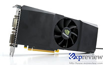
First Single-PCB GeForce GTX 295 Accelerator Spotted
So it is true! NVIDIA does have a single-PCB GeForce GTX 295 accelerator in the works, and partners already seem to have access to it. The card must have had some serious development put into it, given the sheer complexity of the PCB (to cram two G200b GPUs, their display processors, and the PCI-E bridge chip, along with 28 memory chips). The accelerator first surfaced in the form of CAD drawings, in March.
The PCB is pretty straight-forward: populate all the important logic on its business-side, and the memory on either sides. The card maintains its requirement for 8 + 6 pin PCI-E power input. Its VRM is spread across two main areas, to power a GPU system each. Internal SLI connects the two systems, while also providing support for Quad-SLI. Each GPU features 240 shader processors, along with 896 MB of GDDR3 memory across a 448-bit memory interface. Also pictured is the cooler: A fan nucleates the cooler, and blows in two opposite directions. The air is guided by the shroud onto two dense aluminum fin arrays that cool each GPU-system. The back of the card may use a heatspreader to cool the memory, like how the GeForce GTX 280 does it. While we don't expect this design to bring down the retail price of the card, we do believe that the design is mainly to provide partners, and retailers with decent margins that make selling the card a worthwhile venture. With the older design, it might not have been the case.
Source:
Expreview
The PCB is pretty straight-forward: populate all the important logic on its business-side, and the memory on either sides. The card maintains its requirement for 8 + 6 pin PCI-E power input. Its VRM is spread across two main areas, to power a GPU system each. Internal SLI connects the two systems, while also providing support for Quad-SLI. Each GPU features 240 shader processors, along with 896 MB of GDDR3 memory across a 448-bit memory interface. Also pictured is the cooler: A fan nucleates the cooler, and blows in two opposite directions. The air is guided by the shroud onto two dense aluminum fin arrays that cool each GPU-system. The back of the card may use a heatspreader to cool the memory, like how the GeForce GTX 280 does it. While we don't expect this design to bring down the retail price of the card, we do believe that the design is mainly to provide partners, and retailers with decent margins that make selling the card a worthwhile venture. With the older design, it might not have been the case.


75 Comments on First Single-PCB GeForce GTX 295 Accelerator Spotted
I think until Nvidia gets major economical hit they wont understand this strategy of making expensive cards is not the way to go.
I rather Nvidia to keep respawning G92 based cards with minor improvements than to make expensive cards like this.
same coolers as the ones on the palit 4870X2
It has just as many power phases as the original sandwiched GTX295 with each of the three spec'ed for 40A so there's enough juice to go around.
Games stil have to run in SLI mode while the card isnt in seperate 2 PCB ...
They need to re-brand it or somebody dont know if is it single or with 2 PCB...
Or you need always a pic for know what model is...
Well the only advantage that people will buy this card is that it can mount a aftermarket heatsink, which are much more efficient as the original.
Rather than the old model (like mine) would be good if mounted on a waterblock.
This of course if you want silence and overclocking at same time.
I think it's the card that is on top, because the heat tends to rise and the top card holds more heat than the bottom.
That's why the EVGA backplate is a good investiment.
Some people say it is only for aesthetics but for me it helps a lot to cool the upper pcb.
Here's an interesting graph showing the disparity of temperatures for the HD 4870 X2: