Report an Error


AMD Durango
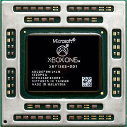
Durango

X871363-001

Die Shot
AMD's Durango GPU uses the GCN 1.0 architecture and is made using a 28 nm production process at TSMC. With a die size of 363 mm² and a transistor count of 5,000 million it is a large chip. Durango supports DirectX 11.2 (Feature Level 11_0). For GPU compute applications, OpenCL version 1.2 can be used. It features 896 shading units, 56 texture mapping units and 16 ROPs.
Graphics Processor
- Released
- Nov 22nd, 2013
- GPU Name
- Durango
- Generation
- Sea Islands
- Architecture
- GCN 1.0
- Foundry
- TSMC
- Process Size
- 28 nm
- Transistors
- 5,000 million
- Density
- 13.8M / mm²
- Die Size
- 363 mm²
- Package
- BGA-1443
Graphics Features
- DirectX
- 11.2 (11_0)
- OpenGL
- N/A
- OpenCL
- 1.2
- Vulkan
- 1.1
- Shader Model
- 5.1
- CLRX
- GCN 1.0.0
Render Config
- Shading Units
- 896
- TMUs
- 56
- ROPs
- 16
- Compute Units
- 14
- Max. TDP
- 95 W
All GCN 1.0 GPUs
AMD GPU Architecture History
- 2024 RDNA 4.0
- 2024 RDNA 3.5
- 2023-2024 CDNA 3.0
- 2022-2024 RDNA 3.0
- 2021 CDNA 2.0
- 2020 CDNA 1.0
- 2020-2023 RDNA 2.0
- 2019-2020 RDNA 1.0
- 2018-2022 GCN 5.1
- 2017-2020 GCN 5.0
- 2016-2020 GCN 4.0
- 2014-2019 GCN 3.0
- 2013-2017 GCN 2.0
- 2011-2020 GCN 1.0
- 2010-2013 TeraScale 3
- 2009-2015 TeraScale 2
- 2005-2013 TeraScale
- 2005-2007 Ultra-Threaded SE
Graphics cards using the AMD Durango GPU
| Name | Chip | Memory | Shaders | TMUs | ROPs | GPU Clock | Memory Clock |
|---|---|---|---|---|---|---|---|
| X871363-001 | 8 GB | 768 | 48 | 16 | 853 MHz | 1066 MHz |

Durango GPU Notes
| Generation: Sea Islands CLRX: GCN 1.0 Instruction issue rate: 12 SCs * 4 SIMDs * 16 threads/clock = 768 ops/clock FLOPs: 768 ops/clock * (1 mul + 1 add) * 800 MHz = 1.2 TFLOPS Interpolation: (768 ops/clock / 2 ops) * 800 MHz = 307.2 Gfloat/sec Triangle rate: 2 tri/clock * 800 MHz = 1.6 Gtri/sec Vertex rate: 2 vert/clock * 800 MHz = 1.6 Gvert/sec Vertex/buffer fetch rate: (4 bytes) 4 elements/clock * 12 SCs * 800 MHz = 38.4 Gelement/sec Vertex/Buffer data rate from cache: 38.4 Gelements/sec * 4 bytes = 153.6 GB/sec Peak throughput from main RAM: 68.2 GB/sec Peak throughput from ESRAM: 128 bytes/clock * 800 MHz = 102.4 GB/sec ESRAM size: 32 MB GSM size: 64 KB LSM size: 12 SCs * 64 KB = 768 KB L2 cache size: 4 x 128 KB = 512 KB (shared) Bilinear fetch rate: (4 bytes) 4 fetches/clock * 12 SCs * 800 MHz = 38.4 Gtexels/sec Bilinear data rate from cache: 38.4 Gtexels/sec * 4 bytes = 153.6 GB/sec L1 cache size: 16 KB/SC * 12 SCs = 192 KB (nonshared) Pixel clear rate: 1 8×8 tile/clock * 4 DBs * 800 MHz = 204.8 Gpixel/sec Pixel hierarchical Z Rate: 1 8×8 tile/clock * 4 DBs * 800 MHz = 204.8 Gpixel/sec Sample Z rate: 16 /clock * 4 DBs * 800 MHz = 51.2 Gsample/sec Pixel rate: 4 /clock * 4 DBs * 800 MHz = 12.8 Gpixel/sec |
Sep 17th, 2024 04:21 EDT
change timezone
Latest GPU Drivers
New Forum Posts
- Ubuntu crontab question (0)
- Which RAM to choose for AMD 7950X3D and keep a 1:1 ratio (33)
- Sapphire pulse rx 7900 gre memory overclock (22)
- Microsoft MUST provide Windows 10 updates for at least another 10 years (23)
- Why everyone say Zen 5 is bad ? (763)
- PC Upgrade (AMD Only) (75)
- What are you playing? (21662)
- Is it easy to damage a PCI-e motherboard slot ? (6)
- G.Skill DDR5 32GB 7600Mhz Trident Z5 Royal - does not work on its frequency! help me figure it out (21)
- Advise me before buying (3)
Popular Reviews
- Warhammer: Space Marine 2 Performance Benchmark Review - 35 GPUs Tested
- Warhammer 40000: Space Marine 2 Handheld Performance Review
- Titan Army P32A2S2 Review - Large Panel, Manageable Resolution
- HYTE Y70 Review
- Upcoming Hardware Launches 2024 (Updated Jul 2024)
- AMD Ryzen 9 9950X Review - The New Flagship
- MOONDROP COSMO Open-Back Planar Magnetic Headphones Review
- AMD Ryzen 7 7800X3D Review - The Best Gaming CPU
- ADATA Legend 970 Pro 2 TB Review
- AMD Radeon RX 7800 XT Review
Controversial News Posts
- AMD Confirms Retreat from the Enthusiast GPU Segment, to Focus on Gaining Market-Share (250)
- Sony Reveals the PlayStation 5 Pro, Launches November 7th (164)
- AnandTech Shuts Down, an Icon of Tech News and Reviews Rides into the Sunset (151)
- AMD Ryzen Branch Prediction Optimizations Now Available to Windows 11 23H2 (130)
- Cyberpunk 2077 Update Adds AMD FSR 3 and Frame Generation for PC Players (118)
- AMD Ryzen 5 7600X3D Launched in the US as a MicroCenter-exclusive for $300, Part of a Bundle (116)
- Report: Intel Could Spin Out Foundry Business or Cancel Some Expansion Plans to Control Losses (113)
- NVIDIA's RTX 5060 "Blackwell" Laptop GPU Comes with 8 GB of GDDR7 Memory Running at 28 Gbps, 25 W Lower TGP (108)