Report an Error


AMD Wimbledon

Wimbledon

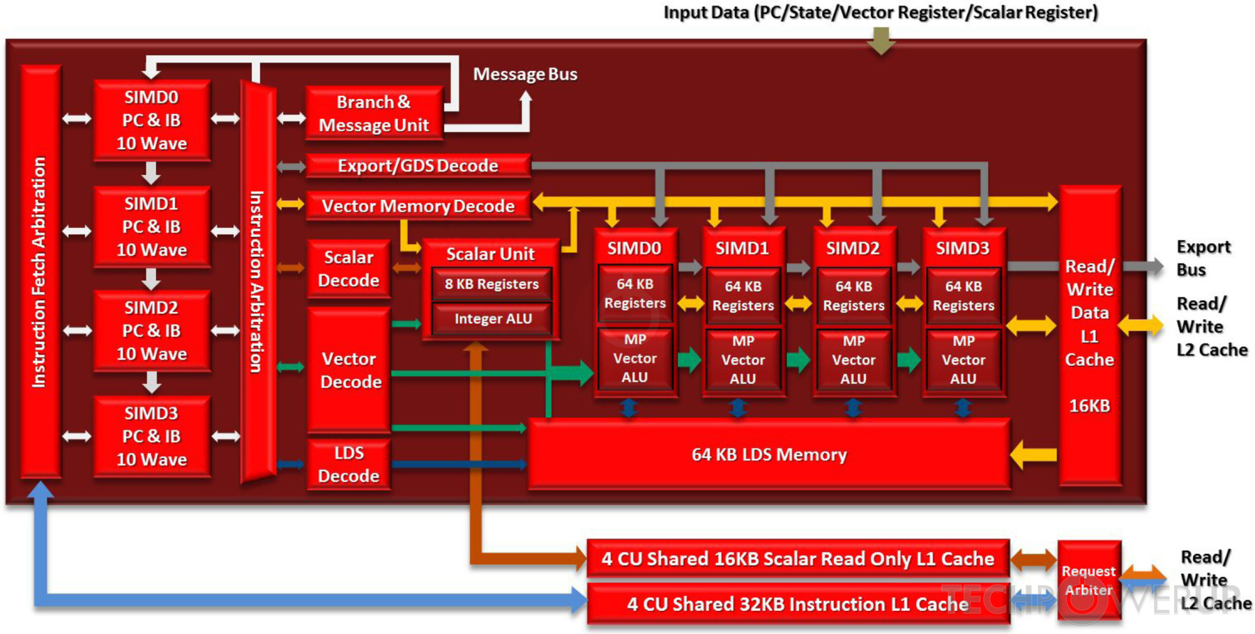
Block Diagram
CU Diagram
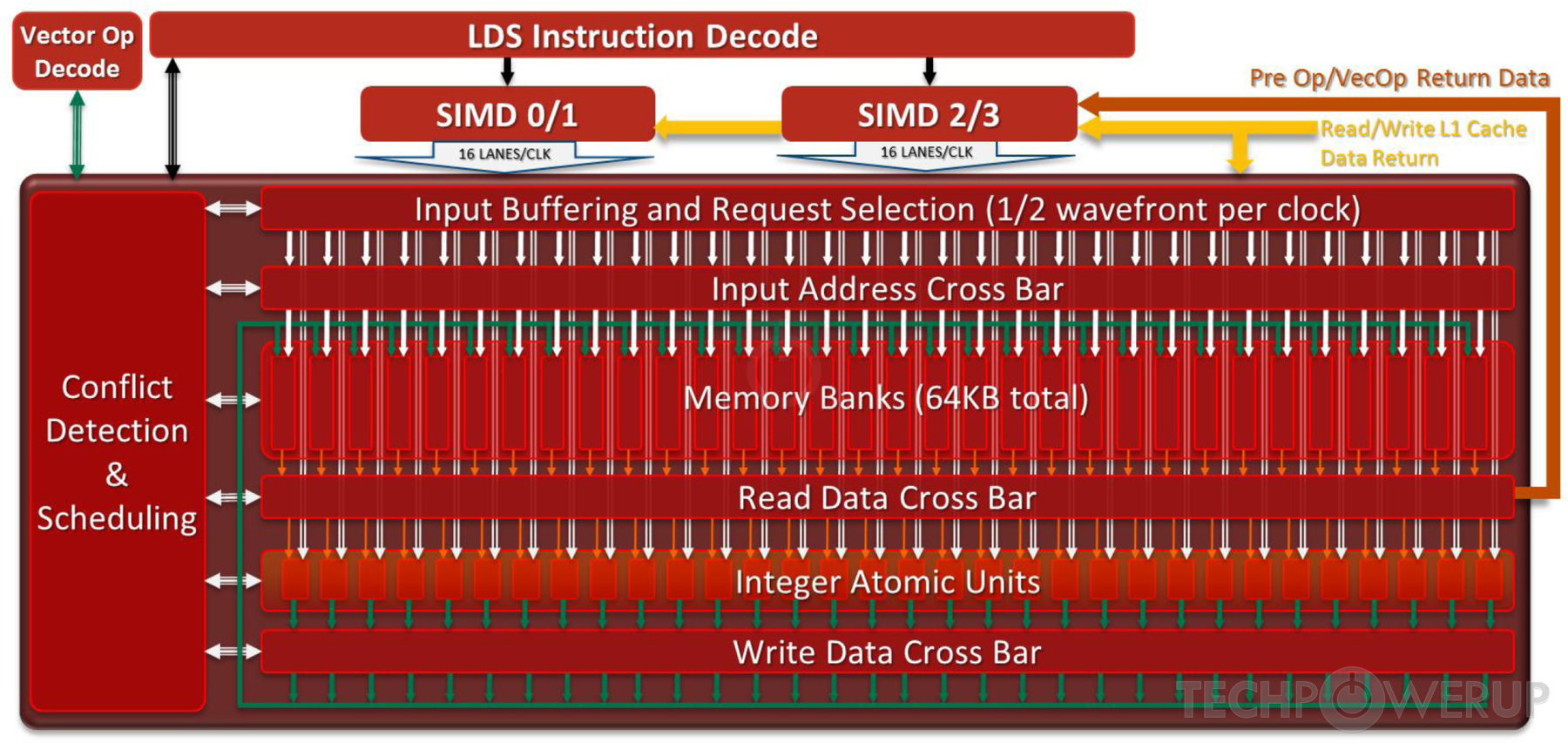
LDS Diagram
AMD's Wimbledon GPU uses the GCN 1.0 architecture and is made using a 28 nm production process at TSMC. With a die size of 212 mm² and a transistor count of 2,800 million it is a medium-sized chip. Wimbledon supports DirectX 12 (Feature Level 11_1). For GPU compute applications, OpenCL version 2.1 (1.2) can be used. It features 1280 shading units, 80 texture mapping units and 32 ROPs.
Further reading:
GCN 1.0 Architecture Whitepaper  , Southern Islands Instruction Set Architecture
Graphics Processor
- Released
- Apr 24th, 2012
- GPU Name
- Wimbledon
- Desktop Variant
- Pitcairn / Curacao
- Mobile Variant
- Neptune
- Generation
- Southern Islands
- Architecture
- GCN 1.0
- Foundry
- TSMC
- Process Size
- 28 nm
- Transistors
- 2,800 million
- Density
- 13.2M / mm²
- Die Size
- 212 mm²
- Package
- FCBGA-1737
Graphics Features
- DirectX
- 12 (11_1)
- OpenGL
- 4.6
- OpenCL
- 2.1 (1.2)
- Vulkan
- 1.2.170
- Shader Model
- 6.5 (5.1)
- WDDM
- 2.7
- Compute
- GFX6 (gfx601)
- DCE
- 6.0
- UVD
- 4.0
- VCE
- 1.0
- CLRX
- GCN 1.0.0
Render Config
- Shading Units
- 1280
- TMUs
- 80
- ROPs
- 32
- Compute Units
- 20
- Z-Stencil
- 128
- ACEs
- 2
- GEs
- 2
- L1 Cache
- 16 KB per CU
- L2 Cache
- 512 KB
- Max. TDP
- 200 W
All GCN 1.0 GPUs
AMD GPU Architecture History
- 2024 RDNA 4.0
- 2024 RDNA 3.5
- 2023-2024 CDNA 3.0
- 2022-2024 RDNA 3.0
- 2021 CDNA 2.0
- 2020 CDNA 1.0
- 2020-2024 RDNA 2.0
- 2019-2020 RDNA 1.0
- 2018-2022 GCN 5.1
- 2017-2020 GCN 5.0
- 2016-2020 GCN 4.0
- 2014-2019 GCN 3.0
- 2013-2017 GCN 2.0
- 2011-2020 GCN 1.0
- 2010-2013 TeraScale 3
- 2009-2015 TeraScale 2
- 2005-2013 TeraScale
- 2005-2007 Ultra-Threaded SE
Graphics cards using the AMD Wimbledon GPU
| Name | Chip | Memory | Shaders | TMUs | ROPs | GPU Clock | Memory Clock |
|---|---|---|---|---|---|---|---|
| Wimbledon XT | 2 GB | 1280 | 80 | 32 | 850 MHz | 1200 MHz | |
| Wimbledon PRO | 2 GB | 1280 | 80 | 32 | 700 MHz | 1000 MHz | |
| Wimbledon XT | 2 GB | 1280 | 80 | 32 | 850 MHz | 1200 MHz |


Wimbledon GPU Notes
| Generation: Southern Islands Desktop Variant: Pitcairn / Curacao / Trinidad Mobile Variant: Wimbledon Graphics/Compute: GFX6 (gfx601) Display Core Engine: 6.0 Unified Video Decoder: 4.0 Video Compression Engine: 1.0 CLRX: GCN 1.0 |
Nov 18th, 2024 05:10 EST
change timezone
Latest GPU Drivers
New Forum Posts
- Anime Nation (12886)
- GPU Test System 2025 Games Selection (3)
- Ghetto Mods (4486)
- ROG version 2.60 windows position (0)
- Technical Issues - TPU Main Site & Forum (2024) (359)
- Upgrade from 13700k to 9800X3D (RAM issues?) (34)
- What Was Your First... (Gaming Related Things) (6)
- Can you split pcie lanes for one device (for example pcie 2.0 x1 to pcie 1.0 x2) (25)
- Linpack Xtreme Released (486)
- What's your latest tech purchase? (22276)
Popular Reviews
- AMD Ryzen 7 9800X3D Review - The Best Gaming Processor
- NVIDIA App v1.0 Review
- Redragon K1NG 8K Review
- Quick Look: MOONDROP Quark2 Type-C In-Ear Monitors
- Valkyrie VK02 Lite Review
- Epomaker TH40 Wireless Mechanical Keyboard Review
- Quick Look: G.SKILL WigiDash PC Command Panel
- Beelink GTi12 Ultra Mini-PC + EX Dock (Intel Core i9-12900H) Review
- Upcoming Hardware Launches 2024 (Updated Nov 2024)
- ASUS GeForce RTX 4060 Dual OC Review - The Best RTX 4060
Controversial News Posts
- AMD Falling Behind: Radeon dGPUs Absent from Steam's Top 20 (222)
- AMD Ryzen 7 9800X3D Stocks Vaporized in Retail, Being Scalped (151)
- AMD Introduces Next-Generation AMD Ryzen 7 9800X3D Processor, $479, Nov 7 (124)
- Apple and Samsung in the Fray to Acquire Intel: Rumor (123)
- AMD Ryzen 7 9800X3D Comes with 120W TDP, 5.20 GHz Boost, All Specs Leaked (120)
- Microsoft Offers $30 Windows 10 Security Extension for Home Users (118)
- AMD Ryzen 7 9800X3D Has the CCD on Top of the 3D V-cache Die, Not Under it (110)
- TechPowerUp is Hiring a Power Supply (PSU) Reviewer (106)