Report an Error


AMD Chelsea

Chelsea
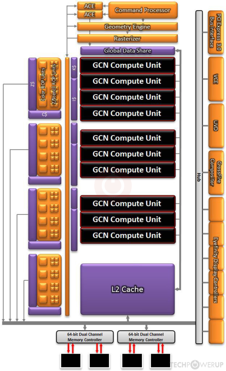
Block Diagram

CU Diagram

LDS Diagram
AMD's Chelsea GPU uses the GCN 1.0 architecture and is made using a 28 nm production process at TSMC. With a die size of 123 mm² and a transistor count of 1,500 million it is a small chip. Chelsea supports DirectX 12 (Feature Level 11_1). For GPU compute applications, OpenCL version 2.1 (1.2) can be used. It features 512 shading units, 32 texture mapping units and 16 ROPs.
Further reading:
GCN 1.0 Architecture Whitepaper  , Southern Islands Instruction Set Architecture
Graphics Processor
- Released
- Apr 24th, 2012
- GPU Name
- Chelsea
- Desktop Variant
- Cape Verde
- Mobile Variant
- Heathrow
- Mobile Variant 2
- Venus / Tropo
- Generation
- Southern Islands
- Architecture
- GCN 1.0
- Foundry
- TSMC
- Package
- FCBGA-962
- Process Size
- 28 nm
- Transistors
- 1,500 million
- Density
- 12.2M / mm²
- Die Size
- 123 mm²
- Package
- FCBGA-962
Graphics Features
- DirectX
- 12 (11_1)
- OpenGL
- 4.6
- OpenCL
- 2.1 (1.2)
- Vulkan
- 1.2.170
- Shader Model
- 6.5 (5.1)
- WDDM
- 2.7
- Compute
- GFX6 (gfx601)
- DCE
- 6.0
- UVD
- 4.0
- VCE
- 1.0
- CLRX
- GCN 1.0.0
Render Config
- Shading Units
- 512
- TMUs
- 32
- ROPs
- 16
- Compute Units
- 8
- Z-Stencil
- 64
- ACEs
- 2
- GEs
- 1
- L1 Cache
- 16 KB per CU
- L2 Cache
- 256 KB
- Max. TDP
- 33 W
All GCN 1.0 GPUs
AMD GPU Architecture History
- 2023 CDNA 3.0
- 2022-2024 RDNA 3.0
- 2021 CDNA 2.0
- 2020 CDNA 1.0
- 2020-2023 RDNA 2.0
- 2019-2020 RDNA 1.0
- 2018-2022 GCN 5.1
- 2017-2020 GCN 5.0
- 2016-2020 GCN 4.0
- 2014-2019 GCN 3.0
- 2013-2017 GCN 2.0
- 2011-2020 GCN 1.0
- 2010-2013 TeraScale 3
- 2009-2015 TeraScale 2
- 2005-2013 TeraScale
- 2005-2007 Ultra-Threaded SE
Graphics cards using the AMD Chelsea GPU
| Name | Chip | Memory | Shaders | TMUs | ROPs | GPU Clock | Memory Clock |
|---|---|---|---|---|---|---|---|
| Chelsea PRO | 1024 MB | 512 | 32 | 16 | 575 MHz | 1000 MHz | |
| Chelsea PRO | 2 GB | 512 | 32 | 16 | 575 MHz | 900 MHz | |
| Chelsea XT | 1024 MB | 512 | 32 | 16 | 675 MHz | 1000 MHz | |
| Chelsea XT GL | 1024 MB | 512 | 32 | 16 | 675 MHz | 1000 MHz |


Chelsea GPU Notes
| Generation: Southern Islands Desktop Variant: Cape Verde Mobile Variant: Heathrow / Venus / Tropo Graphics/Compute: GFX6 (gfx601) Display Core Engine: 6.0 Unified Video Decoder: 4.0 Video Compression Engine: 1.0 CLRX: GCN 1.0 |
Jun 29th, 2024 15:06 EDT
change timezone
Latest GPU Drivers
New Forum Posts
- Samsung 870 EVO - Beware, certain batches prone to failure! (1148)
- The Official Thermal Interface Material thread (1257)
- Power Supply Buying Guide (14)
- RX590 gpu driver for w10 1709-error 184 (6)
- Current Sales, Bundles, Giveaways (10252)
- Forza Horizon 4: Delisting and Removal of All DLC (99)
- Budget PC for Graphic Design (13)
- Memory Mhz importance. (6)
- How to get a internet connection on WINDOWS 2000? (48)
- space between MB chip and GPU (14)
Popular Reviews
- Endgame Gear OP1 8K Review
- Corsair MP600 Mini 2 TB Review - Great Storage for Steam Deck
- Bykski CPU-FIRE-ON-I CPU Water Block Review
- XPG Invader X Review
- Upcoming Hardware Launches 2024 (Updated May 2024)
- Patriot Viper Xtreme 5 DDR5-7600 32 GB CL36 Review
- XFX Radeon RX 7900 XTX Magnetic Air Review
- Lian Li HydroShift LCD 360S AIO Review
- AMD Ryzen 7 7800X3D Review - The Best Gaming CPU
- LAMZU Maya Review - 8000 Hz Tested
Controversial News Posts
- AMD Outs Ryzen 5000XT Processors for Socket AM4, an 8-year Old Socket (208)
- Legendary Overclocker KINGPIN Leaves EVGA and Joins PNY to Develop Next-Generation GPUs for Extreme OC (195)
- AMD Says Ryzen 9000 Series Won't Beat 7000X3D Series at Gaming (140)
- Possible Specs of NVIDIA GeForce "Blackwell" GPU Lineup Leaked (139)
- First Reviews are Live and Snapdragon X Elite Doesn't Quite Deliver on Promised Performance (124)
- ASUS Enhances Customer Support Following Gamers Nexus Investigation (118)
- Nightmare Fuel for Intel: Arm CEO Predicts Arm will Take Over 50% Windows PC Market-share by 2029 (112)
- AMD Zen 5 Storms into Gaming Desktops with Ryzen 9000 "Granite Ridge" Processors (100)