Report an Error


AMD Liverpool

Liverpool
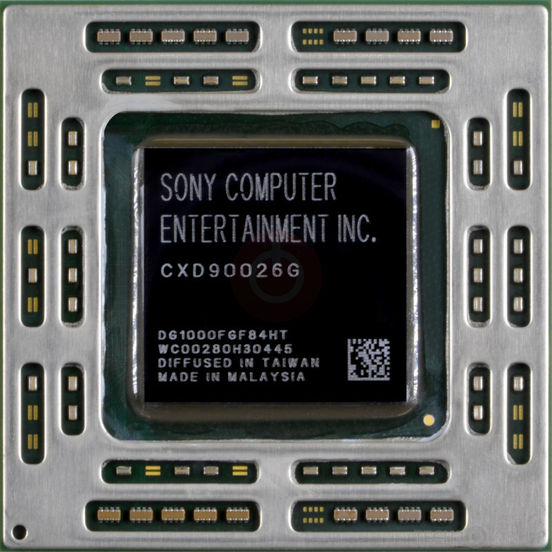
CXD90026G
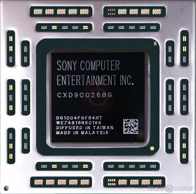
CXD90026BG

CXD90037G

Oleg Kashirin
Die Shot
Block Diagram
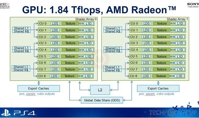
AMD's Liverpool GPU uses the GCN 2.0 architecture and is made using a 28 nm production process at TSMC. With a die size of 348 mm² it is a large chip. Liverpool supports DirectX 11.1*. For GPU compute applications, OpenCL version 1.2 can be used. It features 1152 shading units, 72 texture mapping units and 32 ROPs.
Graphics Processor
- Released
- Nov 24th, 2013
- GPU Name
- Liverpool
- Chip Variant
- Starsha (Thebe-J)
- Generation
- Sea Islands
- Architecture
- GCN 2.0
- Foundry
- TSMC
- Process Size
- 28 nm
- Transistors
- unknown
- Die Size
- 348 mm²
Graphics Features
- DirectX
- 11.1*
- OpenGL
- 4.6
- OpenCL
- 1.2
- Vulkan
- 1.1
- Shader Model
- 5.1
- CLRX
- GCN 1.1.0
Render Config
- Shading Units
- 1152
- TMUs
- 72
- ROPs
- 32
- Compute Units
- 18
- Max. TDP
- 75 W
All GCN 2.0 GPUs
AMD GPU Architecture History
- 2024 RDNA 4.0
- 2024 RDNA 3.5
- 2023-2024 CDNA 3.0
- 2022-2024 RDNA 3.0
- 2021 CDNA 2.0
- 2020 CDNA 1.0
- 2020-2024 RDNA 2.0
- 2019-2020 RDNA 1.0
- 2018-2022 GCN 5.1
- 2017-2020 GCN 5.0
- 2016-2020 GCN 4.0
- 2014-2019 GCN 3.0
- 2013-2017 GCN 2.0
- 2011-2020 GCN 1.0
- 2010-2013 TeraScale 3
- 2009-2015 TeraScale 2
- 2005-2013 TeraScale
- 2005-2007 Ultra-Threaded SE
Graphics cards using the AMD Liverpool GPU
| Name | Chip | Memory | Shaders | TMUs | ROPs | GPU Clock | Memory Clock |
|---|---|---|---|---|---|---|---|
| CXD90026BG | 8 GB | 1152 | 72 | 32 | 800 MHz | 1375 MHz |

Liverpool GPU Notes
| *Supports DirectX 11.1+ Features with PSSL Generation: Sea Islands Codename: Starsha (Thebe-J) CLRX: GCN 1.1.0 |
Oct 18th, 2024 02:59 EDT
change timezone
Latest GPU Drivers
New Forum Posts
- Post your Speedtest.net Speeds! (2308)
- DTS DCH Driver for Realtek HDA [DTS:X APO4 + DTS Interactive] (2002)
- Looking for a a new low power trio for my home studio (43)
- [Detailed + Need Help] Interesting Undervolting Lock(?) Situation on HP Victus 16 r1xxx (5)
- 5700x3d upgrade (3)
- Samsung SSD 860 EVO 250GB - major sudden corruption of random files - advice needed (51)
- installing linux mint with some cinnamon on ssd (3)
- Post your 7-Zip v22.01 scores (397)
- Windows 11 General Discussion (5513)
- Never buy a Crucial P3 plus 4TB SSD (48)
Popular Reviews
- ASRock DeskMini X600 Barebones Mini-PC (Ryzen 8600G) Review
- Corsair 9000D RGB Airflow Review
- 64 Audio Solo Planar Magnetic IEMs Review
- Lian Li O11 Vision Compact Review
- Silent Hill 2 Remake Handheld Performance Review
- Logitech G Pro X Superlight 2 Review - Updated with 8000 Hz Tested
- Silent Hill 2 Remake Performance Benchmark Review - 35 GPUs Tested
- Intel Core Ultra Arrow Lake Preview
- HAVN HS 420 VGPU Review
- Montech King 65 Pro Review
Controversial News Posts
- NVIDIA GeForce RTX 5090 and RTX 5080 Specifications Surface, Showing Larger SKU Segmentation (183)
- AMD Ryzen 9 9950X3D and 9900X3D to Feature 3D V-cache on Both CCD Chiplets (127)
- Quick Denuvo DRM Cracks Cost Game Publishers 20% in Revenue, According to Study (125)
- MSI OCLab Reveals Ryzen 9000X3D 11-13% Faster Than 7000X3D, AMD Set to Dominate "Arrow Lake" in Gaming (123)
- AMD Rushing in Ryzen 7 9800X3D, Expect Product Launch Late-October (117)
- Single-Player Games Lose to PVP in Younger Audiences Despite Recent Hits (116)
- NVIDIA Tunes GeForce RTX 5080 GDDR7 Memory to 32 Gbps, RTX 5070 Launches at CES (112)
- Intel's Core Ultra 9 285K Performance Claims Leaked, Doesn't Beat i9-14900K at Gaming (111)