Report an Error


ATI M28
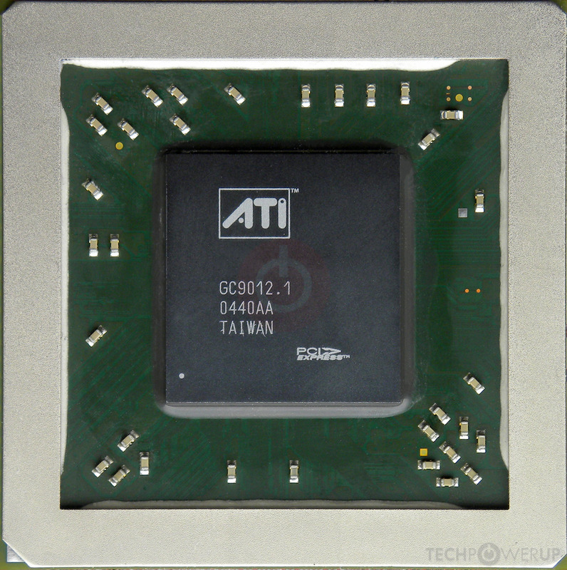
M28

Block Diagram
ATI's M28 GPU uses the R400 architecture and is made using a 130 nm production process at TSMC. With a die size of 289 mm² and a transistor count of 160 million it is a medium-sized chip. M28 supports DirectX 9.0b (Feature Level 9_2). Modern GPU compute technologies are not available. It features 16 pixel shaders and 6 vertex shaders, 16 texture mapping units and 16 ROPs. Due to the lack of unified shaders you will not be able to run recent games at all (which require unified shader/DX10+ support).
Graphics Processor
- Released
- Nov 1st, 2004
- GPU Name
- M28
- Desktop Variant
- R423
- Codename
- Thor
- Architecture
- R400
- Foundry
- TSMC
- Process Size
- 130 nm
- Transistors
- 160 million
- Density
- 553.6K / mm²
- Die Size
- 289 mm²
Graphics Features
- DirectX
- 9.0b (9_2)
- OpenGL
- 2.1
- OpenCL
- N/A
- Vulkan
- N/A
- Pixel Shader
- 2.0b
- Vertex Shader
- 2.0b
- WDDM
- 1.0
- Compute
- GFX2
Render Config
- Pixel Shaders
- 16
- Vertex Shaders
- 6
- TMUs
- 16
- ROPs
- 16
All R400 GPUs
ATI GPU Architecture History
Graphics cards using the ATI M28 GPU
| Name | Chip | Memory | Shaders | TMUs | ROPs | GPU Clock | Memory Clock |
|---|---|---|---|---|---|---|---|
| M28 X800 | 256 MB | 12 / 6 | 12 | 12 | 400 MHz | 400 MHz | |
| M28 X800 XT | 256 MB | 16 / 6 | 16 | 16 | 480 MHz | 550 MHz |


M28 GPU Notes
| Desktop Variant: R423 Codename: Thor Graphics/Compute: GFX2 Smart Shader HD Smooth Vision HD TruForm 2.0 Hyper Z HD Video Shader HD 3Dc Compression Programmable pixel&vertex pipelines |
Nov 20th, 2024 02:19 EST
change timezone
Latest GPU Drivers
New Forum Posts
- Glass mousepad (35)
- [INTEL]-How To Update Your Microcode for Intel HX 13/14th Gen. CPUs Laptops/Mobile Easily. (110)
- whats going on with core 2 quad and windows? (67)
- GPU-Z screenshots not working.. (1)
- Videocard MSI RX 580 ARMOR SP 8 GB (5)
- 9800x 3d vs 12900k - Battle of the Century (133)
- Crazy readings info with GPU-Z on Intel UHD Tiger GT1 (UHD) (4)
- Windows 11 24H2 is driving people to Linux (21)
- X299 Owners Club (86)
- Advise me before buying (98)
Popular Reviews
- NVIDIA SFF-Ready System Build & Benchmark Review - Build Small, Play Big
- AMD Ryzen 7 9800X3D Review - The Best Gaming Processor
- Quick Look: Shanling M1 Plus Portable Audio Player
- Quick Look: MOONDROP Quark2 Type-C In-Ear Monitors
- Valkyrie VK02 Lite Review
- Upcoming Hardware Launches 2024 (Updated Nov 2024)
- NVIDIA App v1.0 Review
- Redragon K1NG 8K Review
- APNX V1-W Review
- DDR5 Memory Performance Scaling with AMD Zen 5
Controversial News Posts
- AMD Falling Behind: Radeon dGPUs Absent from Steam's Top 20 (222)
- AMD Ryzen 7 9800X3D Stocks Vaporized in Retail, Being Scalped (152)
- AMD Introduces Next-Generation AMD Ryzen 7 9800X3D Processor, $479, Nov 7 (124)
- Apple and Samsung in the Fray to Acquire Intel: Rumor (123)
- AMD Ryzen 7 9800X3D Comes with 120W TDP, 5.20 GHz Boost, All Specs Leaked (120)
- Microsoft Offers $30 Windows 10 Security Extension for Home Users (118)
- AMD Ryzen 7 9800X3D Has the CCD on Top of the 3D V-cache Die, Not Under it (110)
- TechPowerUp is Hiring a Power Supply (PSU) Reviewer (105)