Report an Error


AMD Xbox One S GPU
- Graphics Processor
- Durango 2
- Cores
- 768
- TMUs
- 48
- ROPs
- 16
- Memory Size
- 8 GB
- Memory Type
- DDR3
- Bus Width
- 256 bit

GPU

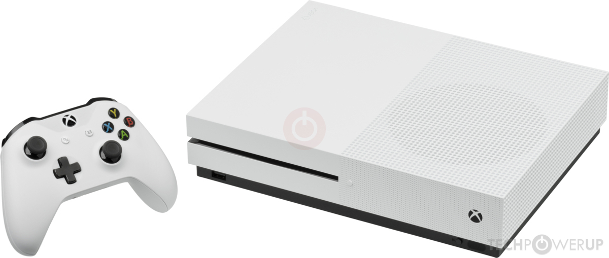
Front 2

Back
Recommended Gaming Resolutions:
- 1600x900
- 1920x1080
- 2560x1440
The Xbox One S GPU was a high-end gaming console graphics solution by AMD, launched on August 2nd, 2016. Built on the 16 nm process, and based on the Durango 2 graphics processor, in its M1004145-001 variant, the device supports DirectX 12. The Durango 2 graphics processor is an average sized chip with a die area of 240 mm² and 5,000 million transistors. It features 768 shading units, 48 texture mapping units, and 16 ROPs. AMD includes 8 GB DDR3 memory, which are connected using a 256-bit memory interface. The GPU is operating at a frequency of 914 MHz, memory is running at 1066 MHz.
Its power draw is rated at 95 W maximum. The console's dimensions are 295 mm x 230 mm x 64 mm, and it features a igp cooling solution. Its price at launch was 399 US Dollars.
Its power draw is rated at 95 W maximum. The console's dimensions are 295 mm x 230 mm x 64 mm, and it features a igp cooling solution. Its price at launch was 399 US Dollars.
Graphics Processor
Graphics Card
- Release Date
- Aug 2nd, 2016
- Generation
-
Console GPU
(Microsoft)
- Production
- End-of-life
- Launch Price
- 399 USD
Clock Speeds
- GPU Clock
- 914 MHz
- Memory Clock
-
1066 MHz
2.1 Gbps effective
Memory
- Memory Size
- 8 GB
- Memory Type
- DDR3
- Memory Bus
- 256 bit
- Bandwidth
- 68.22 GB/s
Render Config
- Shading Units
- 768
- TMUs
- 48
- ROPs
- 16
- Compute Units
- 12
Theoretical Performance
- Pixel Rate
- 14.62 GPixel/s
- Texture Rate
- 43.87 GTexel/s
- FP32 (float)
- 1,404 GFLOPS
Board Design
- Length
- 295 mm
11.6 inches
- Width
- 230 mm
9.1 inches
- Height
- 64 mm
2.5 inches
- Weight
- 2.9 kg (6.4 lbs)
- Storage
- 1 TB HDD
- TDP
- 95 W
- Outputs
- 1x HDMI 2.0a
- Inputs
- 1x HDMI 1.4b
Graphics Features
- DirectX
- 12 (11_1)
- OpenGL
- N/A
- OpenCL
- 1.2
- Vulkan
- 1.1
- Shader Model
- 5.1
Durango 2 GPU Notes
| Generation: Sea Islands Codename: Gladius / Bishop CLRX: GCN 1.0 Instruction issue rate: 12 SCs * 4 SIMDs * 16 threads/clock = 768 ops/clock FLOPs: 768 ops/clock * (1 mul + 1 add) * 914 MHz = 1.404 TFLOPS Interpolation: (768 ops/clock / 2 ops) * 914 MHz = 350.97 Gfloat/sec Triangle rate: 2 tri/clock * 914 MHz = 1.828 Gtri/sec Vertex rate: 2 vert/clock * 914 MHz = 1.828 Gvert/sec Vertex/buffer fetch rate: (4 bytes) 4 elements/clock * 12 SCs * 914 MHz = 43.872 Gelement/sec Vertex/Buffer data rate from cache: 43.872 Gelements/sec * 4 bytes = 175.488 GB/sec Peak throughput from main RAM: 68.2 GB/sec Peak throughput from ESRAM: 128 bytes/clock * 914 MHz = 116.992 GB/sec ESRAM size: 32 MB GSM size: 64 KB LSM size: 12 SCs * 64 KB = 768 KB L2 cache size: 4 x 128 KB = 512 KB (shared) Bilinear fetch rate: (4 bytes) 4 fetches/clock * 12 SCs * 914 MHz = 43.872 Gtexels/sec Bilinear data rate from cache: 43.872 Gtexels/sec * 4 bytes = 175.488 GB/sec L1 cache size: 16 KB/SC * 12 SCs = 192 KB (nonshared) Pixel clear rate: 1 8×8 tile/clock * 4 DBs * 914 MHz = 233.984 Gpixel/sec Pixel hierarchical Z Rate: 1 8×8 tile/clock * 4 DBs * 914 MHz = 233.984 Gpixel/sec Sample Z rate: 16 /clock * 4 DBs * 914 MHz = 58.496 Gsample/sec Pixel rate: 4 /clock * 4 DBs * 914 MHz = 14.624 Gpixel/sec |
May 21st, 2024 10:08 EDT
change timezone
Latest GPU Drivers
New Forum Posts
- For general use - moving files around and playing games, would you have an Optane boot drive or PCie gen 5? (61)
- Ryzen 5 5600x stock overclocked reaching high temps (18)
- AAF Optimus DCH Audio Modded Driver for Windows 10/11 - For ALL HDAUDIO Enumerator Chips (660)
- What are you playing? (20726)
- Kepler BIOS Tweaker problem (0)
- 20 Years? (52)
- Gigabyte am5 motherboard ddr5 not posting when rebooting (0)
- Battery swap for cyberpower UPS (92)
- What's your latest tech purchase? (20607)
- My anti budget PC (60)
Popular Reviews
- Ghost of Tsushima Performance Benchmark Review - 35 GPUs Tested
- Ghost of Tsushima: DLSS vs. FSR vs. XeSS Comparison Review
- PNY XLR8 Gaming EPIC-X RGB DDR5-6400 CL32 32 GB Review
- TerraMaster D8 Hybrid Review
- Silverstone Shark Force 120 mm Fan Review
- Homeworld 3 Performance Benchmark Review - 35 GPUs Tested
- Upcoming Hardware Launches 2023 (Updated Feb 2024)
- Lofree Edge Ultra-Low Profile Wireless Mechanical Keyboard Review
- AMD Ryzen 7 7800X3D Review - The Best Gaming CPU
- AMD Ryzen 7 7700 Review - Affordable Zen 4 Powerhouse
Controversial News Posts
- Intel Statement on Stability Issues: "Motherboard Makers to Blame" (269)
- AMD to Redesign Ray Tracing Hardware on RDNA 4 (227)
- Windows 11 Now Officially Adware as Microsoft Embeds Ads in the Start Menu (173)
- NVIDIA to Only Launch the Flagship GeForce RTX 5090 in 2024, Rest of the Series in 2025 (154)
- AMD Hits Highest-Ever x86 CPU Market Share in Q1 2024 Across Desktop and Server (140)
- AMD RDNA 5 a "Clean Sheet" Graphics Architecture, RDNA 4 Merely Corrects a Bug Over RDNA 3 (139)
- AMD's RDNA 4 GPUs Could Stick with 18 Gbps GDDR6 Memory (114)
- AMD Ryzen 9 7900X3D Now at a Mouth-watering $329 (104)