Report an Error


NVIDIA Quadro 5010M
- Graphics Processor
- GF110
- Cores
- 384
- TMUs
- 48
- ROPs
- 32
- Memory Size
- 4 GB
- Memory Type
- GDDR5
- Bus Width
- 256 bit

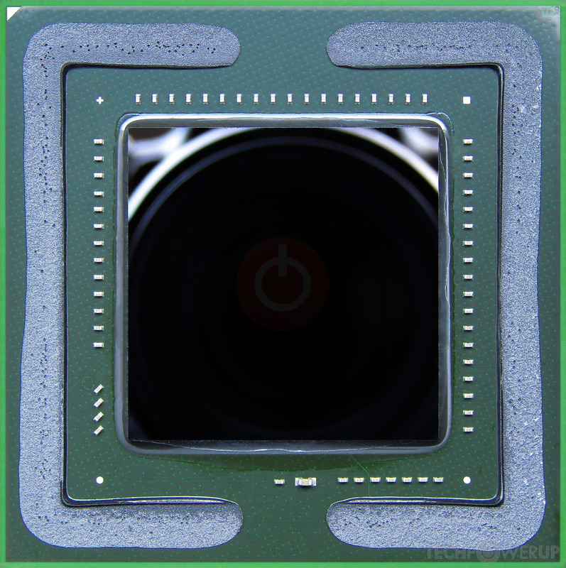
GPU
Recommended Gaming Resolutions:
- 640x480
- 1280x720
- 1366x768
The Quadro 5010M was a professional mobile graphics chip by NVIDIA, launched on February 22nd, 2011. Built on the 40 nm process, and based on the GF110 graphics processor, in its N12E-Q5-A1 variant, the chip supports DirectX 12. The GF110 graphics processor is a large chip with a die area of 520 mm² and 3,000 million transistors. Unlike the fully unlocked GeForce GTX 580, which uses the same GPU but has all 512 shaders enabled, NVIDIA has disabled some shading units on the Quadro 5010M to reach the product's target shader count. It features 384 shading units, 48 texture mapping units, and 32 ROPs. NVIDIA has paired 4 GB GDDR5 memory with the Quadro 5010M, which are connected using a 256-bit memory interface. The GPU is operating at a frequency of 450 MHz, memory is running at 650 MHz (2.6 Gbps effective).
Being a mxm module card, the NVIDIA Quadro 5010M does not require any additional power connector, its power draw is rated at 100 W maximum. This device has no display connectivity, as it is not designed to have monitors connected to it. Rather it is intended for use in laptop/notebooks and will use the output of the host mobile device.
Being a mxm module card, the NVIDIA Quadro 5010M does not require any additional power connector, its power draw is rated at 100 W maximum. This device has no display connectivity, as it is not designed to have monitors connected to it. Rather it is intended for use in laptop/notebooks and will use the output of the host mobile device.
Graphics Processor
Mobile Graphics
- Release Date
- Feb 22nd, 2011
- Generation
-
Quadro Fermi-M
(x000M)
- Predecessor
- Quadro FX Mobile
- Successor
- Quadro Kepler-M
- Production
- End-of-life
- Bus Interface
- MXM-B (3.0)
- Reviews
- 26 in our database
Relative Performance
Based on TPU review data: "Performance Summary" at 1920x1080, 4K for RTX 3080 and faster.
Performance estimated based on architecture, shader count and clocks.
Clock Speeds
- GPU Clock
- 450 MHz
- Shader Clock
- 900 MHz
- Memory Clock
-
650 MHz
2.6 Gbps effective
Memory
- Memory Size
- 4 GB
- Memory Type
- GDDR5
- Memory Bus
- 256 bit
- Bandwidth
- 83.20 GB/s
Render Config
- Shading Units
- 384
- TMUs
- 48
- ROPs
- 32
- SM Count
- 12
- L1 Cache
- 64 KB (per SM)
- L2 Cache
- 512 KB
Theoretical Performance
- Pixel Rate
- 10.80 GPixel/s
- Texture Rate
- 21.60 GTexel/s
- FP32 (float)
- 691.2 GFLOPS
Board Design
- Slot Width
- MXM Module
- TDP
- 100 W
- Outputs
- Portable Device Dependent
- Power Connectors
- None
- Board Number
- P1347 SKU 501
Graphics Features
- DirectX
- 12 (11_0)
- OpenGL
- 4.6
- OpenCL
- 1.1
- Vulkan
- N/A
- CUDA
- 2.0
- Shader Model
- 5.1
GF110 GPU Notes
| PureVideo HD: VP4 VDPAU: Feature Set C GF110 has 4 GPCs each capable of 8 pixels per clock. This limits complete GPU to 32 pixels per clock and because of that it can't feed all 48 ROPs when they all require data at the same time. Additional ROPs however can be used for MSAA (because it doesn't require additional data from rasterizers, while giving more work to ROPs.) The complete die contains 64 texture address units and 256 texture filtering units. Latest Drivers: Windows XP / Server 2003 x64: GeForce Release 368.81 Quadro Release R319 U2 (321.01) Tesla Release 340.62 / R319 U2 (321.01) Windows Vista: GeForce Release 365.19 Quadro Release R346 U7 (348.40) Tesla Release 340.84 Windows 7 / 8 / 8.1 / 10 (x32 / x64): GeForce Release 391.35 Quadro Release R375 U11 (377.83) Tesla Release 340.84 / 412.29 |
Jul 19th, 2025 00:50 CDT
change timezone
Latest GPU Drivers
New Forum Posts
- VMware Workstation is now free for personal use (17)
- What's your latest tech purchase? (24312)
- 9060 XT 8GB or 5060 8GB? (35)
- question for everyone about google play games beta (1)
- Gacha Games - Discussions, Pulls, Updates, etc. (0)
- Idle issue since 5060 ti installed (28)
- Windows 11 General Discussion (6151)
- Have you got pie today? (16795)
- Anime Nation (13054)
- Stalker 2 is looking great. (214)
Popular Reviews
- MSI GeForce RTX 5060 Gaming OC Review
- Razer Blade 16 (2025) Review - Thin, Light, Punchy, and Efficient
- Thermal Grizzly WireView Pro Review
- Pulsar X2 Crazylight Review
- SilverStone SETA H2 Review
- AVerMedia Live Gamer Ultra S (GC553Pro) Review
- Upcoming Hardware Launches 2025 (Updated May 2025)
- Sapphire Radeon RX 9060 XT Pulse OC 16 GB Review - An Excellent Choice
- NVIDIA GeForce RTX 5050 8 GB Review
- Our Visit to the Hunter Super Computer
TPU on YouTube
Controversial News Posts
- Intel's Core Ultra 7 265K and 265KF CPUs Dip Below $250 (288)
- Some Intel Nova Lake CPUs Rumored to Challenge AMD's 3D V-Cache in Desktop Gaming (140)
- AMD Radeon RX 9070 XT Gains 9% Performance at 1440p with Latest Driver, Beats RTX 5070 Ti (131)
- NVIDIA Launches GeForce RTX 5050 for Desktops and Laptops, Starts at $249 (124)
- NVIDIA GeForce RTX 5080 SUPER Could Feature 24 GB Memory, Increased Power Limits (115)
- Microsoft Partners with AMD for Next-gen Xbox Hardware (105)
- NVIDIA DLSS Transformer Cuts VRAM Usage by 20% (99)
- AMD Sampling Next-Gen Ryzen Desktop "Medusa Ridge," Sees Incremental IPC Upgrade, New cIOD (97)