News Posts matching #10 nm SuperFin

Return to Keyword Browsing

Intel "Tiger Lake" Based Pentium and Celeron to Feature AVX2, an Instruction the Entry-Level Brands were Deprived Of

Intel's next-generation Pentium Gold and Celeron entry-level processors based on the "Tiger Lake" microarchitecture could finally receive the AVX2 instruction set. Intel had segmented AVX and AVX2 to be exclusive to the Core and Xeon brands, with the Pentium Gold and Celeron products based on the same microarchitectures to artificially lack these instructions.

Intel updated its ARK product information database with entries for "Tiger Lake" based Pentium Gold and Celeron products. The page for the Pentium Gold 7505 and Celeron 6305, mention support for AVX2 besides SSE4. Both are mobile chips with 15 W TDP, and are built on the same 10 nm SuperFin process as the rest of the 11th Gen Core "Tiger Lake" processor family.

Intel Alder Lake-S CPU Has Been Pictured

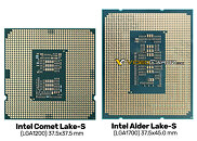
Intel has been preparing the launch of its 10 nm processors for desktop users for some time now, and today we are getting the first pictures of the Alder Lake-S CPU backside. Featuring a package with a size of 37.5×45 mm, the Alder Lake CPU uses more of its area for a pin count increase. Going up from 1200 pins in the LGA1200 socket, the new Alder Lake-S CPU uses 1700 CPU pins, which slots in the LGA1700 socket. In the picture below, there is an engineering sample of the Alder Lake-S CPU, which we see for the first time. While there is no much information about the processor, we know that it will use Intel's 10 nm SuperFin design, paired with hybrid core technology. That means that there will be big (Golden Cove) and little (Gracemont) cores in the design. Other features such as PCIe 5.0 and DDR5 should be present as well. The new CPU generation and LGA1700 motherboards are scheduled to arrive in second half of 2021.

Intel 11th Gen Core "Tiger Lake" & Xe Graphics Launch Event: Live Blog

Intel today launches its 11th Gen Core "Tiger Lake" mobile processors that introduce several new technologies on the backs of new IP. As described in the Architecture Day, "Tiger Lake" is built on the 10 nm SuperFin process, and combines new "Willow Cove" CPU cores with the first commercial debut of the Xe Gen12 graphics architecture that Intel is betting big on, to make a stab at the consumer graphics and scalar compute markets. Join us in this live-blog.

Update 16:00 UTC: GB (Gregory Bryant, EVP Client), leads the event from the comfort of his home.
Update 16:04 UTC: Here it is, the "world's best processor for thin and light laptops. You'll notice that like most Intel U-segment chips, this is an MCM of the processor and PCH die. Intel bases its "world's best" claims on a per-segment basis.

Intel 11th Gen Core "Tiger Lake" Promotional Videos Leak

Promotional videos of Intel 11th Gen Core "Tiger Lake" processors leaked to the web courtesy h0x0d on Twitter. It confirms the new corporate identity of Intel, along with its new logo artistic language. It also confirms the new EVO Powered by Core brand extension, along with a separate case badge for notebooks that use Iris Xe discrete graphics (DG1) in addition to the Xe Gen12 iGPU of "Tiger Lake." Intel has a technology that can get the Xe LP iGPU and dGPU to work in tandem. VideoCardz compiled some interesting frames from the promotional videos, revealing bits such as clock speeds of up to 4.80 GHz (boost), 3.11 GHz (base), the first "Tiger Lake" parts being 4-core/8-thread, the new 10 nm SuperFin transistor, wafer- and die shots of "Tiger Lake" 4c+96EU die, and unless we're mistaken, pictures of a "Tiger Lake" package that uses a DRAM (HBM?) stack on-package, using EMIB. h0x0d also posted videos of the Lenovo Yoga 9i and HP Spectre notebooks based on "Tiger Lake."

Xe HPG is Real, Intel's Gaming GPU Releases in 2021, without HBM

Intel on Thursday at its 2020 Architecture Day event announced a high performance gaming variant of its Xe graphics architecture, which it calls Xe HPG. The Xe architecture is designed to scale between tiny iGPUs and mobile discrete GPUs as Xe LP, up to scalar compute processors under Xe HP, and beyond to HPCs and supercomputers, under Xe HPC. The combination of the client graphics feature-set of Xe LP, with the scale of Xe HP, results in Xe HPG. Intel is designing Xe HPG for a third-party semiconductor foundry, and hopes to debut it in 2021.

In our older graphics detailing the Xe LP, we tried to explain just how easy it is for Intel scale up the iGPU to a discrete GPU SoC. This is done by simply dialing up the Xe slices, and dropping in dGPU ancillaries such as a PCI-Express host interface and memory controllers for the prevalent client-segment discrete graphics, namely GDDR6. There will be additional components, such as ray-tracing hardware. Intel is gunning for DirectX 12 Ultimate logo compliance, and ray-tracing forms a big part of that.

Intel "Willow Cove" Core, Xe LP iGPU, and "Tiger Lake" SoC Detailed

A lot is riding for Intel on its 11th Gen Core "Tiger Lake" system-on-chip (SoC), which will launch exclusively on mobile platforms, hoping to dominate the 7 W thru 15 W ultraportable form-factors in 2020, while eventually scaling up to the 25 W thru 45 W H-segment form-factors in 2021, with a variant that is rumored to double core-counts. The chip is built on Intel's new 10 nm SuperFin silicon fabrication node that enables a double digit percentage energy efficiency growth over 10 nm, allowing Intel to significantly dial up clock speeds without impacting the power envelope. The CPU and iGPU make up the two key components of the "Tiger Lake" SoC.

The CPU component on the "Tiger Lake" processors that launch in a few weeks from now features four "Willow Cove" CPU cores. Coupled with HyperThreading, this ends up being a 4-core/8-thread setup, although much of Intel's innovation is in giving these cores significant IPC increases over the "Skylake" core powering "Comet Lake" processors, and compared to the "Sunny Cove" cores powering "Ice Lake" a minor IPC (although major net performance increase from clock speeds). The "Willow Cove" CPU core appears to be a derivative of the "Sunny Cove" core, designed to take advantage of the 10 nm SuperFin node, along with three key innovations.

Intel 10nm SuperFin Process Goes up Against TSMC 7nm

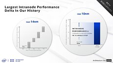
Intel on Thursday made several technological disclosures about its latest silicon fabrication process, the 10 nm SuperFin. With this, the company is changing the nomenclature of its node refinements, away from the ## nm++ naming scheme (with each "+" denoting a refinement, or internode), to a more descriptive naming scheme. The new 10 nm SuperFin node is the first refinement of the company's 10 nm node that debuted with the company's 10th Gen Core "Ice Lake" processors last year, and promises energy efficiency in the ballpark of 7 nm-class nodes by competitors TSMC and Samsung. While past generations of internodes (refinements) delivered energy efficiency improvements of around 3-5%, 10 nm SuperFin offers the kind of improvements expected from a brand new node, according to Intel.

The 10 nm SuperFin node is composed of two key innovations, the SuperMIM capacitor and a redesigned FinFET transistor. The new SuperMIM (metal insulator metal) capacitor offers a 5x increase in capacitance compared to devices in this class. The redesigned FinFET introduces a new barrier that reduces via resistance by 30%. Combined, the 10 nm SuperFin node affords chips a V/F curve comparable to a die-shrink to a whole new silicon fabrication node, without any change in transistor density. The first product built on 10 nm SuperFin is the upcoming Core "Tiger Lake" processor addressing the client-segment. The company is already working on enhancements of this node relevant for data-center processors.
Return to Keyword Browsing
Apr 2nd, 2025 21:22 EDT change timezone

New Forum Posts

Popular Reviews

Controversial News Posts