Apr 6th, 2025 14:22 EDT
change timezone
Latest GPU Drivers
New Forum Posts
- 9070XT or 7900XT (25)
- What local LLM-s you use? (146)
- How I made an Ultimate Cooling Guide (14)
- RX 9000 series GPU Owners Club (191)
- My computer setup - Request for opinions (29)
- Do you use Linux? (558)
- gpu heirarchy/performance/benchmarks- whos lying? (37)
- dropped my xbox controller, now LB doesn't feel clicky (9)
- I have a bricked XFX Radeon RX 580 8GB GPU. HELP! (11)
- Adventure: Running 8/9th gen Coffee Lake CPUs on Z170 motherboard (ASUS Maximus VIII Ranger) (377)
Popular Reviews
- ASUS Prime X870-P Wi-Fi Review
- UPERFECT UStation Delta Max Review - Two Screens In One
- PowerColor Radeon RX 9070 Hellhound Review
- Corsair RM750x Shift 750 W Review
- DDR5 CUDIMM Explained & Benched - The New Memory Standard
- Upcoming Hardware Launches 2025 (Updated Apr 2025)
- Sapphire Radeon RX 9070 XT Pulse Review
- Sapphire Radeon RX 9070 XT Nitro+ Review - Beating NVIDIA
- AMD Ryzen 7 9800X3D Review - The Best Gaming Processor
- Pwnage Trinity CF Review
Controversial News Posts
- MSI Doesn't Plan Radeon RX 9000 Series GPUs, Skips AMD RDNA 4 Generation Entirely (146)
- Microsoft Introduces Copilot for Gaming (124)
- NVIDIA GeForce RTX 5060 Ti 16 GB SKU Likely Launching at $499, According to Supply Chain Leak (124)
- AMD Radeon RX 9070 XT Reportedly Outperforms RTX 5080 Through Undervolting (119)
- NVIDIA Reportedly Prepares GeForce RTX 5060 and RTX 5060 Ti Unveil Tomorrow (115)
- Over 200,000 Sold Radeon RX 9070 and RX 9070 XT GPUs? AMD Says No Number was Given (100)
- NVIDIA GeForce RTX 5050, RTX 5060, and RTX 5060 Ti Specifications Leak (97)
- Nintendo Switch 2 Launches June 5 at $449.99 with New Hardware and Games (92)
News Posts matching #14A
Return to Keyword Browsing
Intel's High-NA EUV Machines Already Processed 30,000 Wafers, More to Come with 14A Node
Intel has successfully deployed two advanced ASML High-NA Twinscan EXE:5000 EUV lithography systems at its D1 development facility near Hillsboro, Oregon, processing approximately 30,000 wafers in a single quarter. The High-NA EUV systems, each reportedly valued at $380 million, represent a substantial improvement over previous lithography tools, achieving resolution down to 8 nm with a single exposure compared to the 13.5 nm resolution of current Low-NA systems. Early operational data indicates these machines are approximately twice as reliable as previous EUV generations, addressing reliability challenges that previously hampered Intel's manufacturing progress. The ability to accomplish with a single exposure what previously required three exposures and approximately 40 processing steps has been reduced to just "single digit" processing steps.
Intel has historically been an early adopter of high-NA EUV lithography, a much more aggressive strategy than its competitors like TSMC, which manufactures its advanced silicon using low-NA EUV tools. The company plans to utilize these systems for its upcoming 14A chip manufacturing process, though no specific mass production date has been announced. While ASML classifies these Twinscan EXE:5000 systems as pre-production tools not designed for high-volume manufacturing, Intel's extensive wafer processing is more of a test bed. The early adoption provides Intel with valuable development opportunities across various High-NA EUV manufacturing aspects, including photomask glass, pellicles, and specialized chemicals that could establish future industry standards. Intel's current 18A node is utilizing Low-NA lithography tools, where Intel is only exploring High-NA with it for testing, before moving on to 14A high-volume manufacturing with High-NA EUV.
Intel has historically been an early adopter of high-NA EUV lithography, a much more aggressive strategy than its competitors like TSMC, which manufactures its advanced silicon using low-NA EUV tools. The company plans to utilize these systems for its upcoming 14A chip manufacturing process, though no specific mass production date has been announced. While ASML classifies these Twinscan EXE:5000 systems as pre-production tools not designed for high-volume manufacturing, Intel's extensive wafer processing is more of a test bed. The early adoption provides Intel with valuable development opportunities across various High-NA EUV manufacturing aspects, including photomask glass, pellicles, and specialized chemicals that could establish future industry standards. Intel's current 18A node is utilizing Low-NA lithography tools, where Intel is only exploring High-NA with it for testing, before moving on to 14A high-volume manufacturing with High-NA EUV.

Intel "Nova Lake" to Appear with up to 52 Cores: 16P+32E+4LPE Configuration
Intel's upcoming "Nova Lake" desktop processors are taking shape slowly, featuring a three-tier core design that could reach 52 total cores. Set for 2026, the flagship SKU combines 16 "Coyote Cove" P-cores with 32 "Arctic Wolf" E-cores, supplemented by 4 LPE-cores for background task management. Intel is reportedly also considering 28-core (8P + 16E + 4LPE), and 16-core (4P + 8E + 4LPE) SKUs too. The architectural design choice centers on Intel's hybrid manufacturing approach, leveraging both its internal 14A node and TSMC's 2 nm process technology. This strategic decision addresses supply chain resilience while potentially enabling higher yields for critical compute tiles. Intel's interim co-CEO Michelle Johnston Holthaus noted that Intel Foundry will need to earn Intel Product's trust with each new node, so if a node is not the best for their in-house IP, Intel will move to TSMC for production.
Initial engineering samples are already circulating among developers, according to shipping documentation from NBD, suggesting the validation phase is proceeding on schedule. Some specifications point to significant cache improvements, with documentation suggesting a 144 MB L3 cache implementation. However, the cache topology—whether unified or segmented—remains unspecified. The platform is expected to support PCIe Gen 6.0, though Intel has yet to confirm socket compatibility or memory specifications. However, we need to hold our expectations low. Previously unrealized configurations in Intel's roadmaps, like 40-core "Arrow Lake," never materialized, and instead, we got an eight-P-core version with 16 E-cores, totaling 24 cores. Final specifications may evolve as the platform progresses through development phases.
Initial engineering samples are already circulating among developers, according to shipping documentation from NBD, suggesting the validation phase is proceeding on schedule. Some specifications point to significant cache improvements, with documentation suggesting a 144 MB L3 cache implementation. However, the cache topology—whether unified or segmented—remains unspecified. The platform is expected to support PCIe Gen 6.0, though Intel has yet to confirm socket compatibility or memory specifications. However, we need to hold our expectations low. Previously unrealized configurations in Intel's roadmaps, like 40-core "Arrow Lake," never materialized, and instead, we got an eight-P-core version with 16 E-cores, totaling 24 cores. Final specifications may evolve as the platform progresses through development phases.

Speculative Intel "Nova Lake" CPU Core Configurations Leaked Online
Intel's freshly uploaded fourth-quarter 2024 "CEO/CFO earnings call comments" document has revealed grand CPU-related plans for 2025 and beyond. One of Team Blue's interim leaders—Michelle Johnston Holthaus—believes that "Nova Lake" processors (a next-generation client family) will arrive in 2026, following a comprehensive rollout of "Panther Lake" CPU products. This official timeline matches previously leaked and rumored development schedules—most notably, in a shipping manifest that was discovered last week. In recent times, industry watchdogs have linked "Nova Lake" to Intel's own 14A node and a TSMC 2 nm process node. Additionally, tipsters pointed to an apparent selection of Coyote Cove performance cores and Arctic Wolf efficiency-oriented cores.
Following yesterday's official announcements, a leaker shared several insights—theorized core configurations and manufacturing details were posted on the Hardware subreddit. Community members were engaged in a debate over Intel's "killing of Falcon Shore," but a plucky contributor—going under the moniker "Exist50"—redirected conversation to all-things "Nova Lake." They believe that Intel has shifted all "compute dies to TSMC" for manufacturing, after a change in plans—initial designs had the "8+16 die" on TSMC's N2P, and the "4+8 die on Intel 18A." Exist50 seemed to have inside track knowledge of product ranges: "Nova Lake (NVL) has a unified HUB/SoC die across mobile and desktop. So yeah, the baseline there is 4+8+4. But there's at least one more die for mobile." The flagship desktop (NVL-S or NVL-SK) chip's configuration could feature as many as sixteen performance cores and thirty-two efficiency cores, due to tile reuse—2x (8P+16E). Exist50 advised Intel CPU enthusiasts to forgo current generation offerings. "Nova Lake" should be: "quite a jump from Arrow Lake (ARL) in terms of MT performance, to say the least. I think anyone who buys ARL will end up regretting it, big time!"

Following yesterday's official announcements, a leaker shared several insights—theorized core configurations and manufacturing details were posted on the Hardware subreddit. Community members were engaged in a debate over Intel's "killing of Falcon Shore," but a plucky contributor—going under the moniker "Exist50"—redirected conversation to all-things "Nova Lake." They believe that Intel has shifted all "compute dies to TSMC" for manufacturing, after a change in plans—initial designs had the "8+16 die" on TSMC's N2P, and the "4+8 die on Intel 18A." Exist50 seemed to have inside track knowledge of product ranges: "Nova Lake (NVL) has a unified HUB/SoC die across mobile and desktop. So yeah, the baseline there is 4+8+4. But there's at least one more die for mobile." The flagship desktop (NVL-S or NVL-SK) chip's configuration could feature as many as sixteen performance cores and thirty-two efficiency cores, due to tile reuse—2x (8P+16E). Exist50 advised Intel CPU enthusiasts to forgo current generation offerings. "Nova Lake" should be: "quite a jump from Arrow Lake (ARL) in terms of MT performance, to say the least. I think anyone who buys ARL will end up regretting it, big time!"


Intel "Nova Lake" Test CPU Appears, Targeting 2026 Launch
Shipping manifests at NBD.ltd have revealed the presence of Intel's "Nova Lake" test chips, providing insight into the development timeline of the company's 2026 processor platform. The discovery comes as Intel prepares for the launch of its "Panther Lake" CPUs on the 18A process node in late 2025. Nova Lake is positioned to replace both Panther Lake for mobile devices and "Arrow Lake" for desktop systems. The manufacturing process remains unconfirmed, with Intel potentially using either its in-house 14A node or TSMC's 2 nm technology. Following recent practices, Intel may split production between its own facilities and TSMC for different components. Rumored specifications show that Nova Lake will use Coyote Cove performance cores and Arctic Wolf efficiency cores.
Unlike Lunar Lake, it will not incorporate on-package memory, maintaining a more conventional design approach. The test chip's appearance suggests Intel is adhering to its development schedule. This timing aligns with the company's plans for Panther Lake's mass production in the second half of 2025, a structured transition between generations. Documents point to "Razor Lake" as Nova Lake's eventual successor, though detailed specifications are not yet available. Panther Lake, the immediate predecessor to Nova Lake, will focus primarily on mobile computing, with desktop variants limited to Mini PC implementations. This approach mirrors the Meteor Lake generation, which saw limited desktop release through the "PS" series for Edge platforms. The Nova Lake platform is expected to support DDR5 memory and may introduce PCIe Gen 6.0 compatibility, with final specifications unconfirmed.
Unlike Lunar Lake, it will not incorporate on-package memory, maintaining a more conventional design approach. The test chip's appearance suggests Intel is adhering to its development schedule. This timing aligns with the company's plans for Panther Lake's mass production in the second half of 2025, a structured transition between generations. Documents point to "Razor Lake" as Nova Lake's eventual successor, though detailed specifications are not yet available. Panther Lake, the immediate predecessor to Nova Lake, will focus primarily on mobile computing, with desktop variants limited to Mini PC implementations. This approach mirrors the Meteor Lake generation, which saw limited desktop release through the "PS" series for Edge platforms. The Nova Lake platform is expected to support DDR5 memory and may introduce PCIe Gen 6.0 compatibility, with final specifications unconfirmed.

Intel Could Manufacture Apple's Next-Generation A20 SoC for iPhone
Apple is reportedly considering diversifying its chip manufacturing strategy with a new silicon manufacturer: Intel. While the upcoming iPhone 17 series, expected next year, will likely feature A19 chips produced by TSMC, a recent rumor from Chinese leaker Fixed Focus Digital hints at a potential switch to Intel for the A20 chipsets powering the 2026 iPhone 18 series. The A18 and A18 Pro chipsets debuted alongside the iPhone 16 series in September 2024, manufactured using TSMC's N3E node. Apple's A19 chips are expected to upgrade to TSMC's N3P node. According to the source, Apple is seeking an Intel 20A node. However, since the A20 node is canceled in favor of 18A, Apple could be an Intel Foundry customer for either 18A or 14A nodes.
Despite the buzz, skepticism persists. Intel has historically struggled with process node transitions and even outsourced production of its Arrow Lake CPUs to TSMC, raising questions about its readiness to deliver on Apple's demands. On the other hand, alternative reports suggest Apple might stick with TSMC's yet-unnamed 2 nm node for the A20, maintaining continuity in its supply chain. As the iPhone 18 series remains two years away, much can change. For now, we are left speculating whether this rumored collaboration with Intel represents a new chapter in Apple's chipset innovation or just a rumor with little substance. If the US government mandates more domestic production, chip designers could be looking at some of the more local manufacturing options, like Intel does on US soil. That could force Apple, NVIDIA, AMD, and Qualcomm to look into Intel's offerings.
Despite the buzz, skepticism persists. Intel has historically struggled with process node transitions and even outsourced production of its Arrow Lake CPUs to TSMC, raising questions about its readiness to deliver on Apple's demands. On the other hand, alternative reports suggest Apple might stick with TSMC's yet-unnamed 2 nm node for the A20, maintaining continuity in its supply chain. As the iPhone 18 series remains two years away, much can change. For now, we are left speculating whether this rumored collaboration with Intel represents a new chapter in Apple's chipset innovation or just a rumor with little substance. If the US government mandates more domestic production, chip designers could be looking at some of the more local manufacturing options, like Intel does on US soil. That could force Apple, NVIDIA, AMD, and Qualcomm to look into Intel's offerings.

Intel and Biden Admin Announce up to $8.5 Billion in Direct Funding Under the CHIPS Act
The Biden-Harris Administration announced today that Intel and the U.S. Department of Commerce have signed a non-binding preliminary memorandum of terms (PMT) for up to $8.5 billion in direct funding to Intel for commercial semiconductor projects under the CHIPS and Science Act. CHIPS Act funding aims to increase U.S. semiconductor manufacturing and research and development capabilities, especially in leading-edge semiconductors. Intel is the only American company that both designs and manufactures leading-edge logic chips. The proposed funding would help advance Intel's critical semiconductor manufacturing and research and development projects at its sites in Arizona, New Mexico, Ohio and Oregon, where the company develops and produces many of the world's most advanced chips and semiconductor packaging technologies.
"Today is a defining moment for the U.S. and Intel as we work to power the next great chapter of American semiconductor innovation," said Intel CEO Pat Gelsinger. "AI is supercharging the digital revolution and everything digital needs semiconductors. CHIPS Act support will help to ensure that Intel and the U.S. stay at the forefront of the AI era as we build a resilient and sustainable semiconductor supply chain to power our nation's future."
"Today is a defining moment for the U.S. and Intel as we work to power the next great chapter of American semiconductor innovation," said Intel CEO Pat Gelsinger. "AI is supercharging the digital revolution and everything digital needs semiconductors. CHIPS Act support will help to ensure that Intel and the U.S. stay at the forefront of the AI era as we build a resilient and sustainable semiconductor supply chain to power our nation's future."

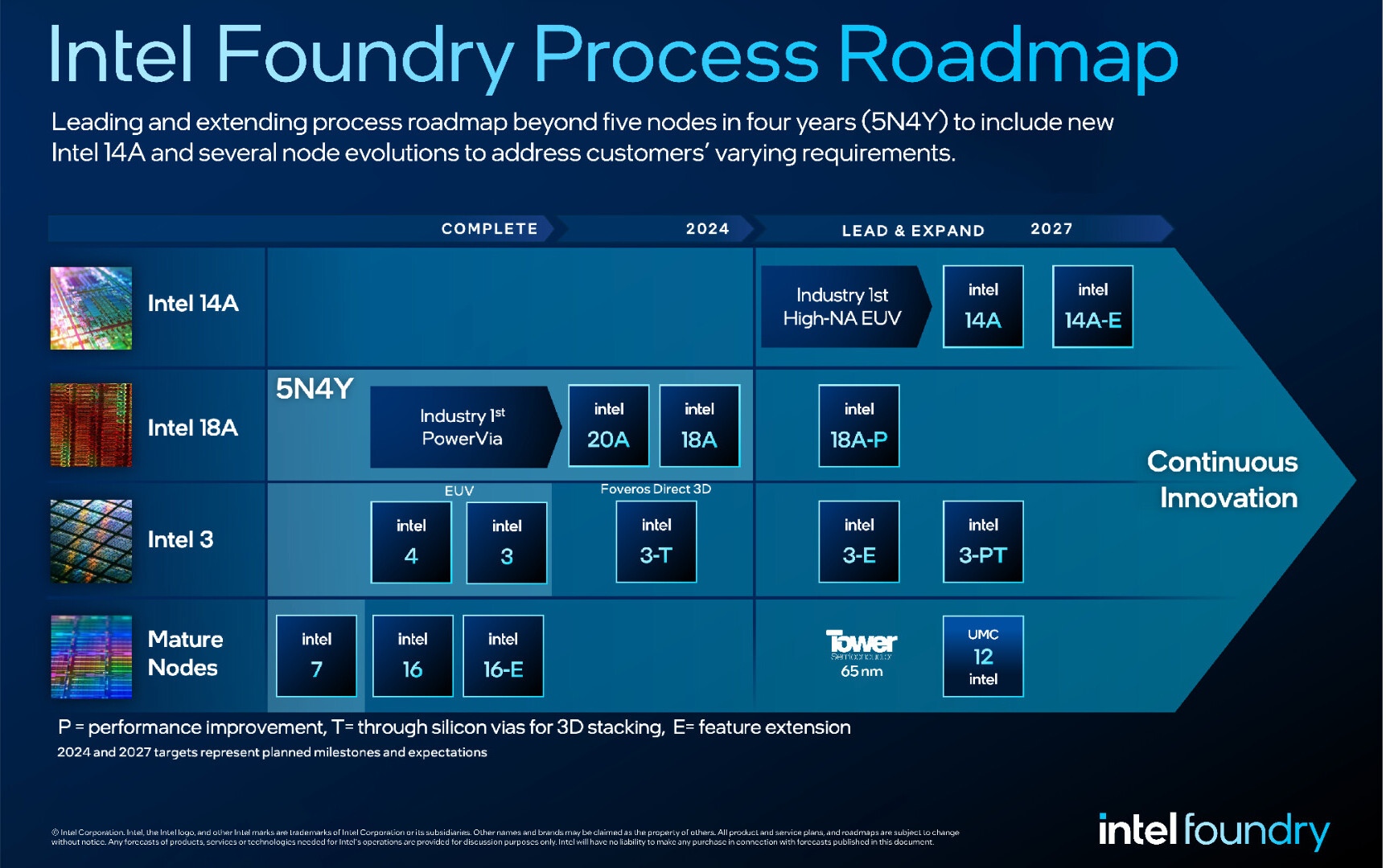
Intel 14A Node Delivers 15% Improvement over 18A, A14-E Adds Another 5%
Intel is revamping its foundry play, and the company is set on its goals of becoming a strong contender to rivals such as TSMC and Samsung. Under Pat Gelsinger's lead, Intel recently split (virtually, under the same company) its units into Intel Product and Intel Foundry. During the SPIE 2024 conference for optics and photonics, Anne Kelleher, Intel's senior vice president, revealed that the 14A (1.4 nm) process offers a 15% performance-per-watt improvement over the company's 18A (1.8 nanometers) process. Additionally, the enhanced 14A-E process boasts a further 5% performance boost from the regular A14 node, being a small refresh. Intel's 14A process is set to be the first to utilize High-NA extreme ultraviolet (EUV) equipment, delivering a 20% increase in transistor logic density compared to the 18A node.
The company's aggressive pursuit of next-generation processes poses a significant threat to Samsung Electronics, which currently holds the second position in the foundry market. As part of its IDM 2.0 strategy, Intel hopes to reclaim its position as a leading foundry player and surpass Samsung by 2030. The company's collaboration with American companies, such as Microsoft, further solidifies its ambitions. Intel has already secured a $15 billion chip production contract with Microsoft for its 1.8 nm 18A process. The semiconductor industry is closely monitoring Intel's progress, as the company's advancements in process technology could potentially reshape the competitive landscape. With Samsung planning to mass-produce 2 nm process products next year, the race for dominance in the foundry market is heating up.

The company's aggressive pursuit of next-generation processes poses a significant threat to Samsung Electronics, which currently holds the second position in the foundry market. As part of its IDM 2.0 strategy, Intel hopes to reclaim its position as a leading foundry player and surpass Samsung by 2030. The company's collaboration with American companies, such as Microsoft, further solidifies its ambitions. Intel has already secured a $15 billion chip production contract with Microsoft for its 1.8 nm 18A process. The semiconductor industry is closely monitoring Intel's progress, as the company's advancements in process technology could potentially reshape the competitive landscape. With Samsung planning to mass-produce 2 nm process products next year, the race for dominance in the foundry market is heating up.


Intel Announces Intel 14A (1.4 nm) and Intel 3T Foundry Nodes, Launches World's First Systems Foundry Designed for the AI Era
Intel Corp. today launched Intel Foundry as a more sustainable systems foundry business designed for the AI era and announced an expanded process roadmap designed to establish leadership into the latter part of this decade. The company also highlighted customer momentum and support from ecosystem partners - including Synopsys, Cadence, Siemens and Ansys - who outlined their readiness to accelerate Intel Foundry customers' chip designs with tools, design flows and IP portfolios validated for Intel's advanced packaging and Intel 18A process technologies.
The announcements were made at Intel's first foundry event, Intel Foundry Direct Connect, where the company gathered customers, ecosystem companies and leaders from across the industry. Among the participants and speakers were U.S. Secretary of Commerce Gina Raimondo, Arm CEO Rene Haas, Microsoft CEO Satya Nadella, OpenAI CEO Sam Altman and others.
The announcements were made at Intel's first foundry event, Intel Foundry Direct Connect, where the company gathered customers, ecosystem companies and leaders from across the industry. Among the participants and speakers were U.S. Secretary of Commerce Gina Raimondo, Arm CEO Rene Haas, Microsoft CEO Satya Nadella, OpenAI CEO Sam Altman and others.
Apr 6th, 2025 14:22 EDT
change timezone
Latest GPU Drivers
New Forum Posts
- 9070XT or 7900XT (25)
- What local LLM-s you use? (146)
- How I made an Ultimate Cooling Guide (14)
- RX 9000 series GPU Owners Club (191)
- My computer setup - Request for opinions (29)
- Do you use Linux? (558)
- gpu heirarchy/performance/benchmarks- whos lying? (37)
- dropped my xbox controller, now LB doesn't feel clicky (9)
- I have a bricked XFX Radeon RX 580 8GB GPU. HELP! (11)
- Adventure: Running 8/9th gen Coffee Lake CPUs on Z170 motherboard (ASUS Maximus VIII Ranger) (377)
Popular Reviews
- ASUS Prime X870-P Wi-Fi Review
- UPERFECT UStation Delta Max Review - Two Screens In One
- PowerColor Radeon RX 9070 Hellhound Review
- Corsair RM750x Shift 750 W Review
- DDR5 CUDIMM Explained & Benched - The New Memory Standard
- Upcoming Hardware Launches 2025 (Updated Apr 2025)
- Sapphire Radeon RX 9070 XT Pulse Review
- Sapphire Radeon RX 9070 XT Nitro+ Review - Beating NVIDIA
- AMD Ryzen 7 9800X3D Review - The Best Gaming Processor
- Pwnage Trinity CF Review
Controversial News Posts
- MSI Doesn't Plan Radeon RX 9000 Series GPUs, Skips AMD RDNA 4 Generation Entirely (146)
- Microsoft Introduces Copilot for Gaming (124)
- NVIDIA GeForce RTX 5060 Ti 16 GB SKU Likely Launching at $499, According to Supply Chain Leak (124)
- AMD Radeon RX 9070 XT Reportedly Outperforms RTX 5080 Through Undervolting (119)
- NVIDIA Reportedly Prepares GeForce RTX 5060 and RTX 5060 Ti Unveil Tomorrow (115)
- Over 200,000 Sold Radeon RX 9070 and RX 9070 XT GPUs? AMD Says No Number was Given (100)
- NVIDIA GeForce RTX 5050, RTX 5060, and RTX 5060 Ti Specifications Leak (97)
- Nintendo Switch 2 Launches June 5 at $449.99 with New Hardware and Games (92)