Imec Demonstrates Logic and DRAM Structures Using High NA EUV Lithography
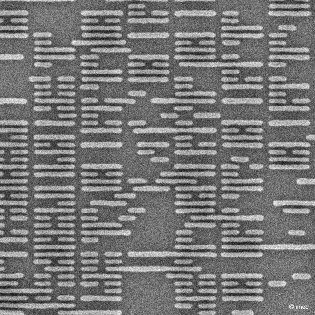
Imec, a world-leading research and innovation hub in nanoelectronics and digital technologies, presents patterned structures obtained after exposure with the 0.55NA EUV scanner in the joint ASML-imec High NA EUV Lithography Lab in Veldhoven, the Netherlands. Random logic structures down to 9,5 nm (19 nm pitch), random vias with 30 nm center-to-center distance, 2D features at 22 nm pitch, and a DRAM specific lay out at P32nm were printed after single exposure, using materials and baseline processes that were optimized for High NA EUV by imec and its partners in the framework of imec's Advanced Patterning Program. With these results, imec confirms the readiness of the ecosystem to enable single exposure high-resolution High NA EUV Lithography.
Following the recent opening of the joint ASML-imec High NA EUV Lithography Lab in Veldhoven, the Netherlands, customers now have access to the (TWINSCAN EXE:5000) High NA EUV scanner to develop private High NA EUV use cases leveraging the customer's own design rules and lay outs.


Following the recent opening of the joint ASML-imec High NA EUV Lithography Lab in Veldhoven, the Netherlands, customers now have access to the (TWINSCAN EXE:5000) High NA EUV scanner to develop private High NA EUV use cases leveraging the customer's own design rules and lay outs.