News Posts matching #3D

Return to Keyword Browsing

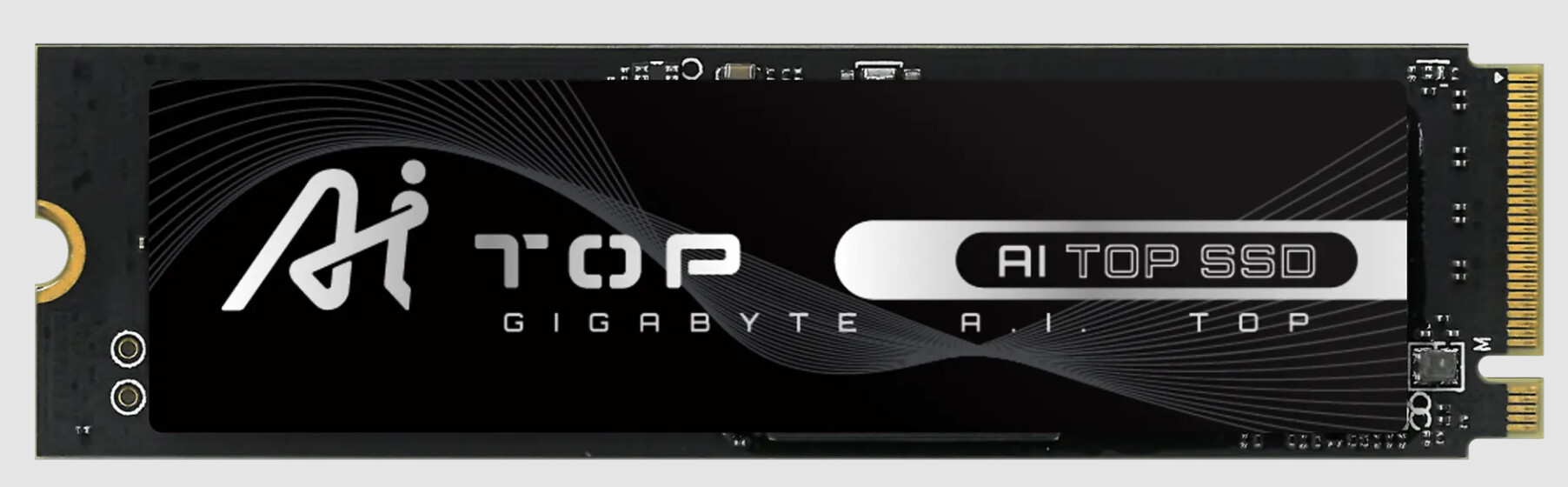
Gigabyte Promises 219,000 TBW for New AI TOP 100E SSD

Gigabyte has quietly added a new SSD to its growing lineup and this time around it's something quite different. The drive is part of Gigabyte's new AI TOP (Trillions of Operations per Second) and was announced at Computex with little fanfare. At the show, the company only announced that it would have 150x the TBW compared to regular SSDs and that it was built specifically for AI model training. What that 150x means in reality is that the 2 TB version of the AI TOP 100E SSD will deliver no less than 219,000 TBW (TeraBytes Written), whereas most high-end 2 TB consumer NVMe SSDs end up somewhere around 1,200 TBW. The 1 TB version promises 109,500 TBW and both drives have an MTBF time of 1.6 million hours and a five-year warranty.

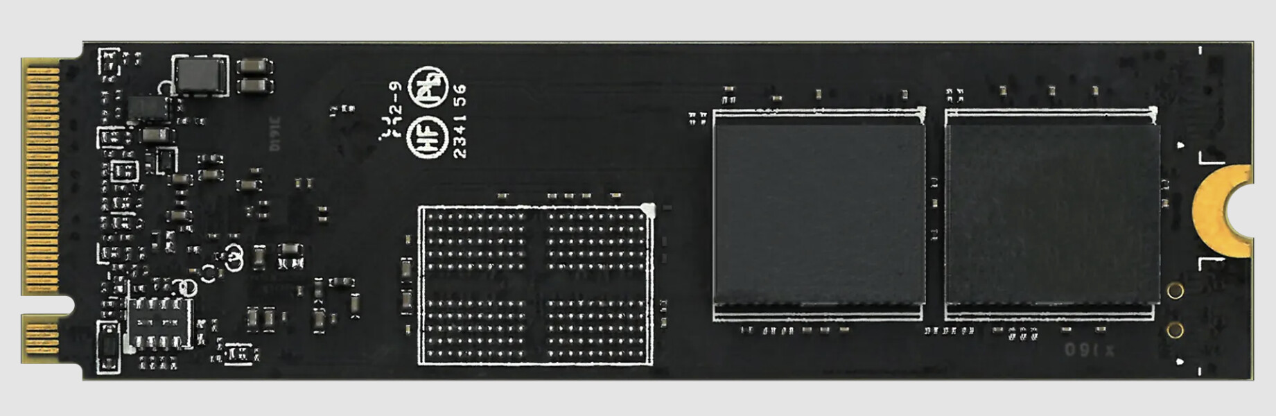
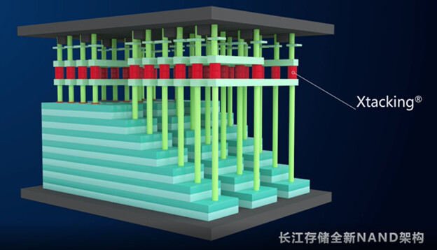
Gigabyte didn't reveal the host controller or the exact NAND used, but the drives are said to use 3D NAND flash and both drives have a LPDDR4 DRAM cache of 1 or 2 GB depending on the drive size. However, the pictures of the drive suggest it might be a Phison based reference design. The AI TOP 100E SSDs are standard PCIe 4.0 drives, so the sequential read speed tops out at 7,200 MB/s with the write speed for the 1 TB SKU being up to 6,500 MB/s, with the 2 TB SKU slightly behind at 5,900 MB/s. No other performance figures were provided. The drives are said to draw up to 11 Watts in use, which seems very high for PCIe 4.0 drives. No word on pricing or availability as yet.

Colorful Presents iGame Lab Project: Highest-Performance GeForce RTX 4090 GPUs Limited to 300 Pieces, OC'd to 3.8 GHz

At Computex 2024, Colorful has launched an ultra-exclusive new graphics card - the iGame Lab 4090. This limited edition GPU is squarely targeted at hardcore overclockers and performance enthusiasts willing to pay top dollar for the absolute best. With only 300 units produced globally, the iGame Lab 4090 represents the pinnacle of Colorful's engineering efforts. Each chip was hand-selected from thousands after rigorous binning to ensure premium silicon capable of extreme overclocks. The card's striking aesthetics feature a clean white shroud with silver accent armor. Beyond the intricate design, the real draw is performance. The iGame Lab 4090 has already shattered records, with professional overclocker CENs pushing it past 3.8 GHz under 3D load. It set a new world record 3DMark Time Spy Extreme score of 24,103 points. Out of the box, the card features a base clock of 2235 MHz, a boost clock of 2520 MHz, and a turbo mode of 2625 MHz, all while being a 3-slot design.

Asetek Announces New AI Optimized Cold Plate Solution In Collaboration With Fabric8Labs

Asetek, innovator of gaming hardware for next-level immersive gaming experiences and the creator of the all-in-one (AIO) liquid cooler, today announced a strategic partnership with Fabric8labs, a leading innovator in metal 3D printing. This exclusive partnership with Fabric8Labs covers the commercial and consumer desktop markets and introduces a revolutionary advancement in liquid cooling technology, showcased in the AI Optimized Cold Plate. Leveraging Fabric8Labs' cutting-edge Electrochemical Additive Manufacturing (ECAM) technology, Asetek has developed a cold plate design that will redefine industry leading performance.

The partnership embodies a shared commitment to innovation that drives superior performance, high quality, and lasting reliability. The AI Optimized Cold Plate demonstrates a significant improvement over previous generations, highlighting the effectiveness of this collaboration. Fabric8Labs' unique 3D printing technology plays a pivotal role in this innovation. Their ECAM method allows for the creation of complex, high-resolution structures that significantly improve thermal capabilities through enhanced fluid dynamics. Also, by eliminating the need for post-processing, ECAM ensures the highest quality and integrity of each cold plate and is massively scalable to support high-volume production demands.

Square Enix Artist Discusses Rebirth's Modernization of Final Fantasy VII 3D Assets

It'd be fair to say Final Fantasy VII Rebirth's next-gen makeover of characters, monsters, and more from the 1997 original has been a spectacular glow-up. The modern console era has returned an iconic cast and world to us with a level of realism in gameplay that even pre-rendered cutscenes over 25 years ago couldn't match. We asked Square Enix if they could crunch some numbers and share some insight into the changes nearly three decades of technological advancement have wrought. Here, main character modeler and lead character artist Dai Suzuki walks us through a selection of characters, creatures, weapons, and more.

Dai Suzuki: When people think of Cloud, most think of his gigantic sword and his unique hairstyle. Because it is so iconic, we needed to put special effort into creating Cloud's hair for Final Fantasy VII Remake, to properly express his personality. The hair was an extremely high-priority element and in fact accounted for half of the total polygon count for the whole model. In Final Fantasy VII Rebirth, the hardware has been changed to PS5, allowing for a higher polygon count to be used than in Final Fantasy VII Remake.

3DMakerpro Officially Launches Moose Series 3D Scanner

3DMakerpro, a pioneer in consumer-friendly 3D scanning technology, announces the launch of the Moose Series, beginner-friendly 3D scanners with AI visual tracking technology. The Moose series is 3DMakerpro's latest consumer-grade 3D scanner line-up offering, designed to handle real-world medium-sized objects into 3D models with remarkable efficiency and precision. Powered by a set of AI features and in collaboration with Oqton, developers of Geomagic Wrap, 3DMakerpro aspires to make 3D scanning easier and more accessible to beginners and advanced users in the creative field.

"The Moose series brings consumer 3D scanning to new heights of accuracy and allows more users to benefit from the convenience of 3D scanning," said Tianshi Yuwen, Global Marketing Director of 3DMakerpro. "Our dedication to innovation empowers us to democratize high-precision 3D scanning and push beyond the boundaries of making all creative visions a reality."

MediaTek Licenses NVIDIA GPU IP for AI-Enhanced Vehicle Processors

NVIDIA has been offering its GPU IP for more than a decade now ever since the introduction of Kepler uArch, and its IP has had relatively low traction in other SoCs. However, that trend seems to be reaching an inflection point as NVIDIA has given MediaTek a license to use its GPU IP to produce the next generation of processors for the auto industry. The newest MediaTek Dimensity Auto Cockpit family consists of CX-1, CY-1, CM-1, and CV-1, where the CX-1 targets premium vehicles, CM targets medium range, and CV targets lower-end vehicles, probably divided by their compute capabilities. The Dimensity Auto Cockpit family is brimming with the latest technology, as the processor core of choice is an Armv9-based design paired with "next-generation" NVIDIA GPU IP, possibly referring to Blackwell, capable of doing ray tracing and DLSS 3, powered by RTX and DLA.

The SoC is supposed to integrate a lot of technology to lower BOM costs of auto manufacturing, and it includes silicon for controlling displays, cameras (advanced HDR ISP), audio streams (multiple audio DSPs), and connectivity (WiFi networking). Interestingly, the SKUs can play movies with AI-enhanced video and support AAA gaming. MediaTek touts the Dimensity Auto Cockpit family with fully local AI processing capabilities, without requiring assistance from outside servers via WiFi, and 3D spatial sensing with driver and occupant monitoring, gaze-aware UI, and natural controls. All of that fits into an SoC fabricated at TSMC's fab on a 3 nm process and runs on the industry-established NVIDIA DRIVE OS.

Canon Wants to Challenge ASML with a Cheaper 5 nm Nanoimprint Lithography Machine

Japanese tech giant Canon hopes to shake up the semiconductor manufacturing industry by shipping new low-cost nanoimprint lithography (NIL) machines as early as this year. The technology, which stamps chip designs onto silicon wafers rather than using more complex light-based etching like market leader ASML's systems, could allow Canon to undercut rivals and democratize leading-edge chip production. "We would like to start shipping this year or next year...while the market is hot. It is a very unique technology that will enable cutting-edge chips to be made simply and at a low cost," said Hiroaki Takeishi, head of Canon's industrial group overseeing nanoimprint lithography technological advancement. Nanoimprint machines target a semiconductor node width of 5 nanometers, aiming to reach 2 nm eventually. Takeishi said the technology has primarily resolved previous defect rate issues, but success will depend on convincing customers that integration into existing fabrication plants is worthwhile.

There is skepticism about Canon's ability to significantly disrupt the market led by ASML's expensive but sophisticated extreme ultraviolet (EUV) lithography tools. However, if nanoimprint can increase yields to nearly 90% at lower costs, it could carve out a niche, especially with EUV supply struggling to meet surging demand. Canon's NIL machines are supposedly 40% the cost of ASML machinery, while operating with up to 90% lower power draw. Initially focusing on 3D NAND memory chips rather than complex processors, Canon must contend with export controls limiting sales to China. But with few options left, Takeishi said Canon will "pay careful attention" to sanctions risks. If successfully deployed commercially after 15+ years in development, Canon's nanoimprint technology could shift the competitive landscape by enabling new players to manufacture leading-edge semiconductors at dramatically lower costs. But it remains to be seen whether the new machines' defect rates, integration challenges, and geopolitical headwinds will allow Canon to disrupt the chipmaking giants it aims to compete with significantly.

Khronos Publishes Vulkan Roadmap 2024, Highlights Expanded 3D Features

Today, The Khronos Group, an open consortium of industry-leading companies creating advanced interoperability standards, announced the latest roadmap milestone for Vulkan, the cross-platform 3D graphics and compute API. The Vulkan roadmap targets the "immersive graphics" market, made up of mid- to high-end smartphones, tablets, laptops, consoles, and desktop devices. The Vulkan Roadmap 2024 milestone captures a set of capabilities that are expected to be supported in new products for that market, beginning in 2024. The roadmap specification provides a significant increase in functionality for the targeted devices and sets the evolutionary direction of the API, including both new hardware capabilities and improvements to the programming model for Vulkan developers.

Vulkan Roadmap 2024 is the second milestone release on the Vulkan Roadmap. Products that support it must be Vulkan 1.3 conformant and support the extensions and capabilities defined in both the 2022 and 2024 Roadmap specifications. Vulkan roadmap specifications use the Vulkan Profile mechanism to help developers build portable Vulkan applications; roadmap requirements are expressed in machine-readable JSON files, and tooling in the Vulkan SDK auto-generates code that makes it easy for developers to query for and enable profile support in their applications.

Paradox Interactive Introduces Prison Architect 2, Breaking Out March 26

Paradox Interactive and Double Eleven have announced Prison Architect 2, the 3D successor to their prison management simulator. The game offers deeper simulation, greater player control, an inhabitant behavior system and creative options to define the next generation of management gameplay. Prison Architect 2 launches on March 26 on Steam, Xbox Series X|S, and PlayStation 5 for a suggested retail price of $39.99 / £34.99 / €39.99. Enterprising Architects can pre-order Prison Architect 2 on PC today.

Prison Architect 2 offers advanced simulation systems, enabling players to construct intricate compounds with a high degree of creative freedom in a 3D environment. From building elaborate structures to managing inmates' needs while maintaining the facility's financial stability, Prison Architect 2 expands gameplay and creative tools across the board, for an engaging sandbox experience. The game also introduces a connection system between the prisoners, who will make friends or enemies with each other, impacting who they will hang out, partner or fight with. Prison Architect 2 brings prison construction and management gameplay to a new level by entering the third dimension and bringing deeper simulation than ever before.

Intel Demos 3D Transistors, RibbonFET, and PowerVia Technologies

During the 69th annual IEEE International Electron Devices Meeting (IEDM), Intel demonstrated some of its latest transistor design and manufacturing advancements. The first one in line is the 3D integration of transistors. According to Intel, the company has successfully stacked complementary field effect transistors (CFET) at a scaled gate pitch down to 60 nm. With CFETs promising thinner gate channels, the 3D stacked CFET would allow for higher density by going vertically and horizontally. Intel's 7 node has a 54 nm gate pitch, meaning CFETs are already close to matching production-ready nodes. With more time and development, we expect to see 3D stacked CFETs in the production runs in the coming years.

Next, Intel has demonstrated RibbonFET technology, a novel approach that is the first new transistor architecture since the introduction of FinFET in 2012. Using ribbon-shaped channels surrounded by the gate, these transistors allow for better control and higher drive current at all voltage levels. This allows faster transistor switching speeds, which later lead to higher frequency and performance. The width of these nanoribbon channels can be modulated depending on the application, where low-power mobile applications use less current, making the channels thinner, and high-performance applications require more current, making the channels wider. One stack of nanoribbons can achieve the same drive current as multiple fins found in FinFET but at a smaller footprint.

YMTC Develops 128 and 232-Layer Xtacking 4.0 NAND Memory Chips

Chinese memory maker Yangtze Memory Technology Corp (YMTC) is allegedly preparing its next-generation Xtacking 4.0 3D NAND flash architecture for next-generation memory chips. According to the documentation obtained by Tom's Hardware, YMTC has developed two SKUs based on the upgraded Xtacking 4.0: X4-9060, a 128-layer three-bit-per-cell (TLC) 3D NAND, and the X4-9070, a 232-layer TLC 3D NAND. By using string stacking on both of these SKUs, YMTC plans to make the 3D NAND work by incorporating arrays with 64 and 116 active layers stacked on top of each other. This way, the export regulation rules from the US government are met, and the company can use the tools that are not under the sanction list.

While YMTC has yet to fully disclose the specific advantages of the Xtacking 4.0 technology, the industry anticipates significant enhancements in data transfer speeds and storage density. These improvements are expected to stem from increased plane counts for optimized parallel processing, refined bit/word line configurations to minimize latency, and the development of modified chip variants to boost production yields. When YMTC announced Xtacking 3.0, the company offered 128-layer TLC and 232-layer four-bit-per-cell (QLC) variants and was the first company to achieve 200+ layer count in the 3D NAND space. The Xtacking 3.0 architecture incorporates string stacking and hybrid bonding techniques and uses a mature process node for the chip's CMOS underlayer. We have to wait for the final Xtacking 4.0 details when YMTC's officially launches the SKUs.

TYAN Announces New Server Line-Up Powered by 4th Gen AMD EPYC (9004/8004 Series) and AMD Ryzen (7000 Series) Processors at SC23

TYAN, an industry leader in server platform design and a subsidiary of MiTAC Computing Technology Corporation, debuts its new server line-up for 4th Gen AMD EPYC & AMD Ryzen Processors at SC23, Booth #1917, in the Colorado Convention Center, Denver, CO, November 13-16.

AMD EPYC 9004 processor features leadership performance and is optimized for a wide range of HPC, cloud-native computing and Generative AI workloads
TYAN offers server platforms supporting the AMD EPYC 9004 processors that provide up to 128 Zen 4C cores and 256 MB of L3 Cache for dynamic cloud-native applications with high performance, density, energy efficiency, and compatibility.

3Dconnexion Releases New SpaceMouse Pro Wireless - Bluetooth Edition

3Dconnexion, a leader in innovative input devices for professionals, is thrilled to announce the launch of the highly anticipated SpaceMouse Pro Wireless Bluetooth Edition. Purpose-built for engineers, 3D artists and architects, the new SpaceMouse Pro Wireless delivers a seamless experience centered on sustainability and meeting the evolving needs of professionals worldwide.

The SpaceMouse Pro Wireless Bluetooth Edition embodies 3Dconnexion's commitment to excellence and environmental responsibility, adding new features to the ones that professionals have been trusting and relying on for years.

Rambus Boosts AI Performance with 9.6 Gbps HBM3 Memory Controller IP

Rambus Inc., a premier chip and silicon IP provider making data faster and safer, today announced that the Rambus HBM3 Memory Controller IP now delivers up to 9.6 Gigabits per second (Gbps) performance supporting the continued evolution of the HBM3 standard. With a 50% increase over the HBM3 Gen 1 data rate of 6.4 Gbps, the Rambus HBM3 Memory Controller can enable a total memory throughput of over 1.2 Terabytes per second (TB/s) for training of recommender systems, generative AI and other demanding data center workloads.

"HBM3 is the memory of choice for AI/ML training, with large language models requiring the constant advancement of high-performance memory technologies," said Neeraj Paliwal, general manager of Silicon IP at Rambus. "Thanks to Rambus innovation and engineering excellence, we're delivering the industry's leading-edge performance of 9.6 Gbps in our HBM3 Memory Controller IP."

Zero ASIC Democratizing Chip Making

Zero ASIC, a semiconductor startup, came out of stealth today to announce early access to its one-of-a-kind ChipMaker platform, demonstrating a number of world firsts:
  • 3D chiplet composability enabling billions of new silicon products
  • Fully automated no-code chiplet-based chip design
  • Zero install interactive RTL-based chip emulation
  • Roadmap to 100X reduction in chip development costs
"Custom Application Specific Integrated Circuits (ASICs) offer 10-100X cost and energy advantage over commercial off the shelf (COTS) devices, but the enormous development cost makes ASICs non-viable for most applications," said Andreas Olofsson, CEO and founder of Zero ASIC. "To build the next wave of world changing silicon devices, we need to reduce the barrier to ASICs by orders of magnitude. Our mission at Zero ASIC is to make ordering an ASIC as easy as ordering catalog parts from an electronics distributor."

Samsung Notes: HBM4 Memory is Coming in 2025 with New Assembly and Bonding Technology

According to the editorial blog post published on the Samsung blog by SangJoon Hwang, Executive Vice President and Head of the DRAM Product & Technology Team at Samsung Electronics, we have information that High-Bandwidth Memory 4 (HBM4) is coming in 2025. In the recent timeline of HBM development, we saw the first appearance of HBM memory in 2015 with the AMD Radeon R9 Fury X. The second-generation HBM2 appeared with NVIDIA Tesla P100 in 2016, and the third-generation HBM3 saw the light of the day with NVIDIA Hopper GH100 GPU in 2022. Currently, Samsung has developed 9.8 Gbps HBM3E memory, which will start sampling to customers soon.

However, Samsung is more ambitious with development timelines this time, and the company expects to announce HBM4 in 2025, possibly with commercial products in the same calendar year. Interestingly, the HBM4 memory will have some technology optimized for high thermal properties, such as non-conductive film (NCF) assembly and hybrid copper bonding (HCB). The NCF is a polymer layer that enhances the stability of micro bumps and TSVs in the chip, so memory solder bump dies are protected from shock. Hybrid copper bonding is an advanced semiconductor packaging method that creates direct copper-to-copper connections between semiconductor components, enabling high-density, 3D-like packaging. It offers high I/O density, enhanced bandwidth, and improved power efficiency. It uses a copper layer as a conductor and oxide insulator instead of regular micro bumps to increase the connection density needed for HBM-like structures.

Fujitsu Details Monaka: 150-core Armv9 CPU for AI and Data Center

Ever since the creation of A64FX for the Fugaku supercomputer, Fujitsu has been plotting the development of next-generation CPU design for accelerating AI and general-purpose HPC workloads in the data center. Codenamed Monaka, the CPU is the latest creation for TSMC's 2 nm semiconductor manufacturing node. Based on Armv9-A ISA, the CPU will feature up to 150 cores with Scalable Vector Extensions 2 (SVE2), so it can process a wide variety of vector data sets in parallel. Using a 3D chiplet design, the 150 cores will be split into different dies and placed alongside SRAM and I/O controller. The current width of the SVE2 implementation is unknown.

The CPU is designed to support DDR5 memory and PCIe 6.0 connection for attaching storage and other accelerators. To bring cache coherency among application-specific accelerators, CXL 3.0 is present as well. Interestingly, Monaka is planned to arrive in FY2027, which starts in 2026 on January 1st. The CPU will supposedly use air cooling, meaning the design aims for power efficiency. Additionally, it is essential to note that Monaka is not a processor that will power the post-Fugaku supercomputer. The post-Fugaku supercomputer will use post-Monaka design, likely iterating on the design principles that Monaka uses and refining them for the launch of the post-Fugaku supercomputer scheduled for 2030. Below are the slides from Fujitsu's presentation, in Japenese, which highlight the design goals of the CPU.

Acer's New SpatialLabs View Pro 27 Display Elevates Glasses-Free Stereoscopic 3D Experiences

Acer unveiled its largest and most advanced glasses-free stereoscopic 3D display to date, the Acer SpatialLabs View Pro 27. Crafted as a state-of-the-art 3D canvas for creators and developers, the display elevates the way ideas and audiovisual elements take shape without needing specialized glasses or accessories. The device is powered by SpatialLabs's proven stereoscopic 3D solution and is complimented by the new Acer Immerse Audio system, along with a suite of advanced developer tools to bring out creations in their truest 3D forms. Users can also fully maximize its vast 27-inch 4K panel for magnified, lifelike visuals, while its ergonomic design and detachable hood provide comfortable viewing even under extremely low-light conditions.

Expanded Design for Mesmerizing 3D Illustrations
The Acer SpatialLabs View Pro 27 harmoniously combines cutting-edge 3D technology and stereo real-time rendering capabilities in an expanded landscape to support creators in bringing 3D experiences to life. The optimized 3D display uses an eye-tracking module to follow the position and movement of users in real-time even in dim environments. Crystal-clear details and image depth are projected as envisioned thanks to its 27-inch 4K UHD display with 2D and 3D modes, allowing users to switch between 2D and 3D stereoscopic views, along with the panel's 160 Hz refresh rate, 400 nits brightness, Delta E< 2 color accuracy. A detachable hood on the monitor enhances perceived color accuracy and lessens distractions, helping users stay focused and maintain image quality when viewing their designs on screen.

TSMC Announces Breakthrough Set to Redefine the Future of 3D IC

TSMC today announced the new 3Dblox 2.0 open standard and major achievements of its Open Innovation Platform (OIP) 3DFabric Alliance at the TSMC 2023 OIP Ecosystem Forum. The 3Dblox 2.0 features early 3D IC design capability that aims to significantly boost design efficiency, while the 3DFabric Alliance continues to drive memory, substrate, testing, manufacturing, and packaging integration. TSMC continues to push the envelope of 3D IC innovation, making its comprehensive 3D silicon stacking and advanced packaging technologies more accessible to every customer.

"As the industry shifted toward embracing 3D IC and system-level innovation, the need for industry-wide collaboration has become even more essential than it was when we launched OIP 15 years ago," said Dr. L.C. Lu, TSMC fellow and vice president of Design and Technology Platform. "As our sustained collaboration with OIP ecosystem partners continues to flourish, we're enabling customers to harness TSMC's leading process and 3DFabric technologies to reach an entirely new level of performance and power efficiency for the next-generation artificial intelligence (AI), high-performance computing (HPC), and mobile applications."

Synopsys and TSMC Streamline Multi-Die System Complexity with Unified Exploration-to-Signoff Platform and Proven UCIe IP on TSMC N3E Process

Synopsys, Inc. today announced it is extending its collaboration with TSMC to advance multi-die system designs with a comprehensive solution supporting the latest 3Dblox 2.0 standard and TSMC's 3DFabric technologies. The Synopsys Multi-Die System solution includes 3DIC Compiler, a unified exploration-to-signoff platform that delivers the highest levels of design efficiency for capacity and performance. In addition, Synopsys has achieved first-pass silicon success of its Universal Chiplet Interconnect Express (UCIe) IP on TSMC's leading N3E process for seamless die-to-die connectivity.

"TSMC has been working closely with Synopsys to deliver differentiated solutions that address designers' most complex challenges from early architecture to manufacturing," said Dan Kochpatcharin, head of the Design Infrastructure Management Division at TSMC. "Our long history of collaboration with Synopsys benefits our mutual customers with optimized solutions for performance and power efficiency to help them address multi-die system design requirements for high-performance computing, data center, and automotive applications."

Intel Unveils Industry-Leading Glass Substrates to Meet Demand for More Powerful Compute

What's New: Intel today announced one of the industry's first glass substrates for next-generation advanced packaging, planned for the latter part of this decade. This breakthrough achievement will enable the continued scaling of transistors in a package and advance Moore's Law to deliver data-centric applications.

"After a decade of research, Intel has achieved industry-leading glass substrates for advanced packaging. We look forward to delivering these cutting-edge technologies that will benefit our key players and foundry customers for decades to come."
-Babak Sabi, Intel senior vice president and general manager of Assembly and Test Development

AMD Reports Second Quarter 2023 Financial Results, Revenue Down 18% YoY

AMD today announced revenue for the second quarter of 2023 of $5.4 billion, gross margin of 46%, operating loss of $20 million, net income of $27 million and diluted earnings per share of $0.02. On a non-GAAP basis, gross margin was 50%, operating income was $1.1 billion, net income was $948 million and diluted earnings per share was $0.58.

"We delivered strong results in the second quarter as 4th Gen EPYC and Ryzen 7000 processors ramped significantly," said AMD Chair and CEO Dr. Lisa Su. "Our AI engagements increased by more than seven times in the quarter as multiple customers initiated or expanded programs supporting future deployments of Instinct accelerators at scale. We made strong progress meeting key hardware and software milestones to address the growing customer pull for our data center AI solutions and are on-track to launch and ramp production of MI300 accelerators in the fourth quarter."

NVIDIA Key Player in Creation of OpenUSD Standard for 3D Worlds

NVIDIA joined Pixar, Adobe, Apple and Autodesk today to found the Alliance for OpenUSD, a major leap toward unlocking the next era of 3D graphics, design and simulation. The group will standardize and extend OpenUSD, the open-source Universal Scene Description framework that's the foundation of interoperable 3D applications and projects ranging from visual effects to industrial digital twins.

Several leading companies in the 3D ecosystem already signed on as the alliance's first general members—Cesium, Epic Games, Foundry, Hexagon, IKEA, SideFX and Unity. Standardizing OpenUSD will accelerate its adoption, creating a foundational technology that will help today's 2D internet evolve into a 3D web. Many companies are already working with NVIDIA to pioneer this future.

ASUS Republic of Gamers Announces ROG Strix SCAR 17 X3D, the World's First AMD Ryzen 9 7945HX3D Laptop

ASUS Republic of Gamers (ROG) today announced the new ROG Strix SCAR 17 X3D, the perfect fusion of cutting-edge silicon and ROG engineering. Featuring the AMD Ryzen 9 7945HX3D mobile processor equipped with AMD 3D V-Cache technology for the very first time, the Strix SCAR 17 X3D takes performance to a whole new level. By doubling the L3 cache of the mighty Ryzen 9 7945HX processor, the Ryzen 9 7945HX3D gives users a boost in games that are hungry for this onboard ultrafast memory. Paired with a 240 Hz QHD display, Conductonaut Extreme liquid metal on the GPU, and a vapor chamber, the Strix SCAR 17 X3D is ready to dominate the leaderboards.

Making great processors even better
While the original 2023 ROG Strix SCAR 17 came equipped with AMD Ryzen 7000 Series processors, the AMD Ryzen 9 7945HX3D is truly in a league of its own. It leverages the power of AMD 3D V-Cache technology, a stacking of extra ultra-high-speed L3 cache vertically on top of one of the two core compute dies (CCD). This extra cache enables the eight cores to perform certain calculations quickly and efficiently, notably in gaming. For situations where increasing CPU frequency simply doesn't show significant performance gains, 3D V-Cache technology holds the potential to unlock extra compute power.

NEO Semiconductor to Present Its Ground-Breaking 3D NAND and 3D DRAM Architectures at Flash Memory Summit 2023

NEO Semiconductor, a leading developer of innovative technologies for 3D NAND flash and DRAM memory, today announced its participation at Flash Memory Summit 2023, taking place in person in Santa Clara, California, on August 8-10. CEO, Andy Hsu, will deliver a keynote address titled "New Architectures which will Drive Future 3D NAND and 3D DRAM Solutions" on August 9th at 11:40 a.m. Pacific Time.

Earlier this year, Neo Semiconductor announced the launch of its ground-breaking technology, 3D X-DRAM. This development is the world's first 3D NAND-like DRAM cell array that is targeted to solve DRAM's capacity bottleneck and replace the entire 2D DRAM market. 3D X-DRAM can be manufactured using the existing 3D NAND flash memory process with minor changes, significantly reducing the time and cost spent developing a new 3D process. During the keynote, Mr. Hsu will reveal the 3D X-DRAM process flow and technical details.
Return to Keyword Browsing
Jul 16th, 2024 01:28 EDT change timezone

New Forum Posts

Popular Reviews

Controversial News Posts