News Posts matching #4 nm

Return to Keyword Browsing

MSI Announces New Features and Support for AMD Ryzen 9000 Series Processors

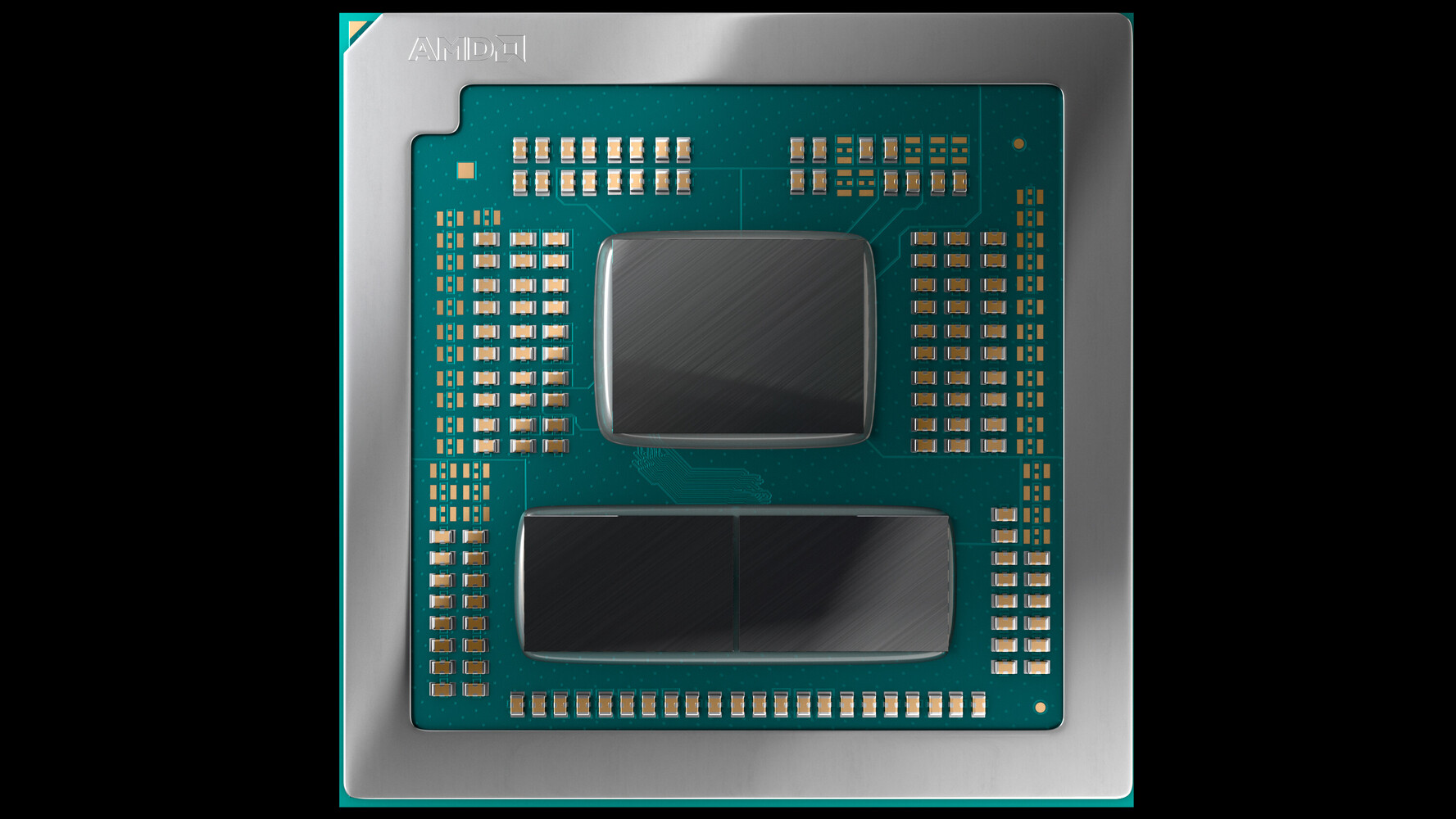
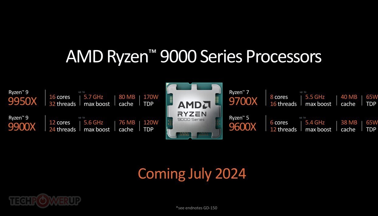
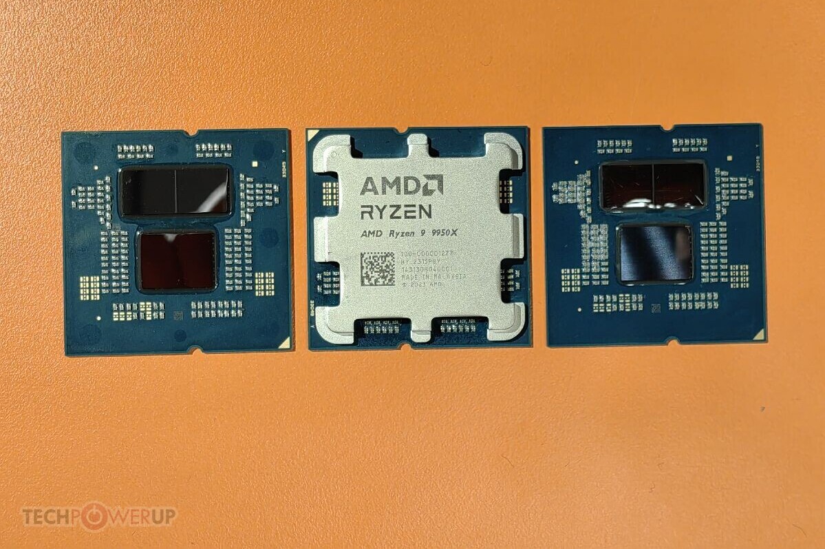
MSI is excited to announce the launch of the latest AMD Ryzen 9000 Series processors, set to debut on the AM5 platform. Powered by advanced 4 nm CPU process technology, the Ryzen 9000 Series promises to revolutionize the computing landscape with unmatched performance, efficiency, and versatility for gamers and content creators. At launch, August 8th, AMD Ryzen 7 9700X, and Ryzen 5 9600X are available while the Ryzen 9 9950X and 9900X will launch on August 15th. These processors will feature up to 16 cores and 32 threads, with a theoretical maximum boost clock speed of 5.7 GHz, 64 MB of L3 cache, and a maximum TDP of 170 W.

AMD Ryzen 9000 Series will also support PCIe 5.0 for the GPU and M.2 while enhancing DDR5 memory speed. Notably, the AMD Ryzen 7 9700X offers approximately 12% better overall performance than the first-gen AMD 3D V-cache CPU. All these processors are compatible with the AM5 socket, and existing AMD 600 Series motherboards and Ryzen 9000 Series processors can seamlessly integrate by updating to the latest BIOS, available on MSI's product support page.

AMD Strix Point Silicon Pictured and Annotated

The first die shot of AMD's new 4 nm "Strix Point" mobile processor surfaced, thanks to an enthusiast on Chinese social media. "Strix Point" is a significantly larger die than "Phoenix." It measures 12.06 mm x 18.71 mm (L x W), compared to the 9.06 mm x 15.01 mm of "Phoenix." Much of this die size increase comes from the larger CPU, iGPU, and NPU. The process has been improved from TSMC N4 on "Phoenix" and its derivative "Hawk Point," to the newer TSMC N4P node.

Nemez (GPUsAreMagic) annotated the die shot in great detail. The CPU now has 12 cores spread across two CCX, one of which contains four "Zen 5" cores sharing a 16 MB L3 cache; and the other with eight "Zen 5c" cores sharing an 8 MB L3 cache. The two CCXs connect to the rest of the chip over Infinity Fabric. The rather large iGPU takes up the central region of the die. It is based on the RDNA 3.5 graphics architecture, and features 8 workgroup processors (WGPs), or 16 compute units (CU) worth 1,024 stream processors. Other key components include four render backends worth 16 ROPs, and control logic. The GPU has its own 2 MB of L2 cache that cushions transfers to the Infinity Fabric.

AMD Ryzen "Fire Range" Mobile Processor Retains FL1 Package

AMD is readying a successor to its Ryzen 7045 series "Dragon Range" mobile processor for gaming notebooks and portable workstations. While we don't know its processor model naming yet, the chip is codenamed "Fire Range." We are learning that it will retain the FL1 package as "Dragon Range," which means it will be pin-compatible. This would significantly reduce development costs for notebook OEMs, as they can simply carry over their mainboard designs from their notebooks based on "Dragon Range."

"Fire Range" is essentially a mobile BGA version of the upcoming Ryzen 9000 "Granite Ridge" desktop processor. The FL1 package measures 40 mm x 40 mm in size, and has substrate for two CCDs and a cIOD, just like the desktop chip. "Fire Range" hence features one or two 4 nm "Zen 5" CCDs, depending on the processor model, and the 6 nm client I/O die. Much like "Dragon Range," the "Fire Range" chip will lack support for LPDDR5, and rely on conventional PC DDR5 memory in the SO-DIMM or CAMM2 form-factors. Besides the CPU core count consisting exclusively of full-sized "Zen 5" cores, the main flex for "Fire Range" over "Strix Point" will be its 28-lane PCIe Gen 5 root-complex, which can wire out the fastest discrete mobile GPUs, as well as drive multiple M.2 NVMe slots with Gen 5 wiring, and other high-bandwidth devices, such as Thunderbolt 4, USB4, or Wi-Fi 7 controllers wired directly to the processor.

Ryzen 9000 Chip Layout: New Details Announced

AMD "Granite Ridge" is codename for the four new Ryzen 9000 series desktop processors the company plans to launch on July 31, 2024. The processor is built in the Socket AM5 package, and is meant to be backwards compatible with AMD 600-series chipset motherboards, besides the new 800-series chipset ones that will launch alongside. "Granite Ridge" is a chiplet-based processor, much like the Ryzen 7000 "Raphael," Ryzen 5000 "Vermeer," and Ryzen 3000 "Matisse." AMD is carrying over the 6 nm client I/O die over from "Raphael" in an effort to minimize development costs, much in the same way it carried over the 12 nm cIOD for "Vermeer" from "Matisse."

The SoC I/O features of "Granite Ridge" are contemporary, with its awesome 28-lane PCI-Express Gen 5 root complex that allows a PCI-Express 5.0 x16, two CPU-attached M.2 Gen 5 slots, and a Gen 5 x4 chipset bus. There's also a basic integrated graphics solution based on the older RDNA 2 graphics architecture; which should make these processors fit for all use-cases that don't need discrete graphics. The iGPU even has multimedia accelerators, an audio coprocessor, a display controller, and USB 3.2 interfaces from the processor.

Avnet ASIC Team Launches Ultra-Low-Power Design Services for TSMC's 4nm Process Nodes

Avnet ASIC, a division of Avnet Silica, an Avnet company, today announced that it has launched its new ultra-low-power design services for TSMC's cutting-edge 4 nm and below process technologies. These services are designed to enable customers to achieve exceptional power efficiency and performance in their high-performance applications, such as blockchain and AI edge computing. TSMC is the world's leading silicon foundry and Avnet ASIC division is a leading provider of ASIC and SoC full turnkey solutions.

The new design services leverage a comprehensive approach to address the challenges of operating at extreme low-voltage conditions in the 4 nm and below nodes. This includes recharacterizing standard cells for lower voltages, performing early RTL exploration to optimize power, performance, and area (PPA) tradeoffs, implementing an optimized clock tree, and utilizing transistor-level simulations to enhance the power optimization process.

NVIDIA GeForce "Blackwell" Won't Arrive Before January 2025?

It appears like 2024 will go down as the second consecutive year without any new GPU generation launch from either NVIDIA or AMD. Kopite7kimi, a reliable source with NVIDIA leaks, says that the GeForce RTX 50-series "Blackwell" generation won't see a debut before the 2025 International CES (January 2025). It was earlier expected that the company would launch at least its top two SKUs—the RTX 5090 and RTX 5080—toward the end of 2024, and ramp the series up from 2025. There is no explanation behind this "delay." Like everyone else, NVIDIA could be rationing its foundry allocation of the 3 nm wafers from TSMC for its high-margin "Blackwell" AI GPUs. The company now makes over five times the revenue from selling AI GPUs than it does from gaming GPUs, so this development should come as little surprise.

Things aren't any different with NVIDIA's rivals in this space, AMD and Intel. AMD's RDNA 4 graphics architecture and the Radeon RX series GPUs based on it, aren't expected to arrive before 2025. AMD is making several architectural upgrades with RDNA 4, particularly to its ray tracing hardware; and the company is expected to build these GPUs on a new foundry node. Meanwhile, Intel's Arc B-series gaming GPUs based on the Xe2 "Battlemage" graphics architecture are expected to arrive in 2025, too, although these chips are rumored to be based on a more mature 4 nm-class foundry node.

AMD Granite Ridge and Strix Point Zen 5 Die-sizes and Transistor Counts Confirmed

AMD is about give the new "Zen 5" microarchitecture a near-simultaneous launch across both its client segments—desktop and mobile. The desktop front is held by the Ryzen 9000 "Granite Ridge" Socket AM5 processors; while Ryzen AI 300 "Strix Point" powers the company's crucial effort to capture Microsoft Copilot+ AI PC market share. We recently did a technical deep-dive on the two. HardwareLuxx.de scored two important bits of specs for both processors in its Q&A interaction with AMD—die sizes and transistor counts.

To begin with, "Strix Point" is a monolithic silicon, which is confirmed to be built on the TSMC N4P foundry node (4 nm). This is a slight upgrade over the N4 node that the company built its previous generation "Phoenix" and "Hawk Point" processors on. The "Strix Point" silicon measures 232.5 mm² in area, which is significantly larger than the 178 mm² of "Hawk Point" and "Phoenix." The added die area comes from there being 12 CPU cores instead of 8, and 16 iGPU compute units instead of 12; and a larger NPU. There are many other factors, such as the larger 24 MB CPU L3 cache; and the sizes of the "Zen 5" and "Zen 5c" cores themselves.

TSMC to Raise Wafer Prices by 10% in 2025, Customers Seemingly Agree

Taiwanese semiconductor giant TSMC is reportedly planning to increase its wafer prices by up to 10% in 2025, according to a Morgan Stanley note cited by investor Eric Jhonsa. The move comes as demand for cutting-edge processors in smartphones, PCs, AI accelerators, and HPC continues to surge. Industry insiders reveal that TSMC's state-of-the-art 4 nm and 5 nm nodes, used for AI and HPC customers such as AMD, NVIDIA, and Intel, could see up to 10% price hikes. This increase would push the cost of 4 nm-class wafers from $18,000 to approximately $20,000, representing a significant 25% rise since early 2021 for some clients and an 11% rise from the last price hike. Talks about price hikes with major smartphone manufacturers like Apple have proven challenging, but there are indications that modest price increases are being accepted across the industry. Morgan Stanley analysts project a 4% average selling price increase for 3 nm wafers in 2025, which are currently priced at $20,000 or more per wafer.

Mature nodes like 16 nm are unlikely to see price increases due to sufficient capacity. However, TSMC is signaling potential shortages in leading-edge capacity to encourage customers to secure their allocations. Adding to the industry's challenges, advanced chip-on-wafer-on-substrate (CoWoS) packaging prices are expected to rise by 20% over the next two years, following previous increases in 2022 and 2023. TSMC aims to boost its gross margin to 53-54% by 2025, anticipating that customers will absorb these additional costs. The impact of these price hikes on end-user products remains uncertain. Competing foundries like Intel and Samsung may seize this opportunity to offer more competitive pricing, potentially prompting some chip designers to consider alternative manufacturing options. Additionally, TSMC's customers could reportedly be unable to secure their capacity allocation without "appreciating TSMC's value."

AMD "Strix Halo" a Large Rectangular BGA Package the Size of an LGA1700 Processor

Apparently the AMD "Strix Halo" processor is real, and it's large. The chip is designed to square off against the likes of the Apple M3 Pro and M3 Max, in letting ultraportable notebooks have powerful graphics performance. A chiplet-based processor, not unlike the desktop socketed "Raphael," and mobile BGA "Dragon Range," the "Strix Halo" processor consists of one or two CCDs containing CPU cores, wired to a large die, that's technically the cIOD (client I/O die), but containing an oversized iGPU, and an NPU. The point behind "Strix Halo" is to eliminate the need for a performance-segment discrete GPU, and conserve its PCB footprint.

According to leaks by Harukaze5719, a reliable source with AMD leaks, "Strix Halo" comes in a BGA package dubbed FP11, measuring 37.5 mm x 45 mm, which is significantly larger than the 25 mm x 40 mm size of the FP8 BGA package that the regular "Strix Point," "Hawk Point," and "Phoenix" mobile processors are built on. It is larger in area than the 40 mm x 40 mm FL1 BGA package of "Dragon Range" and upcoming "Fire Range" gaming notebook processors. "Strix Halo" features one or two of the same 4 nm "Zen 5" CCDs featured on the "Granite Ridge" desktop and "Fire Range" mobile processors, but connected to a much larger I/O die, as we mentioned.

Intel Arc Xe2 "Battlemage" Discrete GPUs Made on TSMC 4 nm Process

Intel has reportedly chosen the TSMC 4 nm EUV foundry node for its next generation Arc Xe2 discrete GPUs based on the "Battlemage" graphics architecture. This would mark a generational upgrade from the Arc "Alchemist" family, which Intel built on the TSMC 6 nm DUV process. The TSMC N4 node offers significant increases in transistor densities, performance, and power efficiency over the N6, which is allowing Intel to nearly double the Xe cores on its largest "Battlemage" variant in numerical terms. This, coupled with increased IPC, clock speeds, and other features, should make the "Battlemage" contemporary against today's AMD RDNA 3 and NVIDIA Ada gaming GPUs. Interestingly, TSMC N4 isn't the most advanced foundry node that the Xe2 "Battlemage" is being built on. The iGPU powering Intel's Core Ultra 200V "Lunar Lake" processor is part of its Compute tile, which Intel is building on the more advanced TSMC N3 (3 nm) node.

ASUS to Host AI PC Event on July 17, to Launch Nine Designs Based on AMD Ryzen AI 300

ASUS announced a press event on July 17 to launch at least nine notebook designs powered by AMD Ryzen AI 300 series "Strix Point" mobile processors. All these notebooks are AI PCs that meet Microsoft Copilot+ requirements. Each of the 9 designs will have several variants based on the processor model, discrete graphics, and other hardware differentiators, making up dozens of individual SKUs. The AMD "Strix Point" mobile processor is based on a 4 nm monolithic die. It combines a 12-core/24-thread CPU based on a combination of "Zen 5" and "Zen 5c" cores, a 50 TOPS-class NPU, and a powerful iGPU based on the RDNA 3.5 graphics architecture, with 16 compute units.

Among the notebook designs ASUS plans to announce on July 17 are the ROG Zephyrus G16 (GA605), the TUF Gaming A14 (FA401), the TUF Gaming A16 (FA608), the Zenbook S16 (UM5606), Vivobook S14 (M5406), Vivobook S16 (M5506 and M5606), ProArt P16 (HN7606) and ProArt PX13 (HN7306). With these, ASUS is covering pretty much all its notebook market segments, including enthusiast gaming, performance gaming, boutique ultraportability, mainstream, and creative professional.

DDR5-6400 Confirmed as Sweetspot Speed of Ryzen 9000 "Zen 5" Desktop Processors

AMD's upcoming Ryzen 9000 series "Granite Ridge" desktop processors based on the "Zen 5" microarchitecture will see a slight improvement in memory overclocking capabilities. A chiplet-based processor, just like the Ryzen 7000 "Raphael," "Granite Ridge" combines one or two "Zen 5" CCDs, each built on the TSMC 4 nm process, with a client I/O die (cIOD) built on the 6 nm node. The cIOD of "Granite Ridge" appears to be almost identical to that of "Raphael." This is the chiplet that contains the processor's DDR5 memory controllers.

As part of the update, Ryzen 9000 "Granite Ridge" should be able to run DDR5-6400 with a 1:1 ratio between the MCLK and FCLK domains. This is a slight increase from the DDR5-6000 sweetspot speed of Ryzen 7000 "Raphael" processors. AMD is reportedly making it possible for motherboard manufacturers and prebuilt OEMs to enable a 1:2 ratio, making it possible to run high memory speeds such as DDR5-8000, although performance returns with memory speeds would begin to diminish beyond the DDR5-6400 @ 1:1 setting. Memory manufacturers should launch a new wave of DDR5 memory kits with AMD EXPO profiles for DDR5-6400.

AMD to Revise Specs of Ryzen 7 9700X to Increase TDP to 120W, to Beat 7800X3D

AMD's Ryzen 9000 "Granite Ridge" family of Socket AM5 desktop processors based on the "Zen 5" microarchitecture arrive in July, with four processor models in the lead—the 9950X 16-core, the 9900X 12-core, the 9700X 8-core, and the 9600X 6-core. AMD is building the CCDs (CPU core dies) of these processors on the slightly newer 4 nm foundry node, compared to the 5 nm node that the Ryzen 7000 series "Raphael" processors based on "Zen 4" are built on; and generally lowered the TDP values of all but the top 16-core part. The company is reportedly reconsidering these changes, particularly in wake of company statements that the 9000X series may not beat the 7000X3D series in gaming performance, which may have sullied the launch, particularly for gamers.

From the company's Computex 2024 announcement of the Ryzen 9000 series, the 9950X has the same 170 W TDP as its predecessor, the 7950X. The 9900X 12-core part, however, comes with a lower 120 W TDP compared to the 170 W of the 7900X. Things get interesting with the 8-core and 6-core parts. Both the 9700X 8-core, and the 9600X 6-core chips come with 65 W TDP. The 9700X succeeds the 7700X, which came with a 105 W TDP, while the 9600X succeeds the 7600X that enjoys the same 105 W TDP. The TDP and package power tracing (PPT) values of an AMD processor are known to affect CPU boost frequency residence, particularly in some of the higher core-count SKUs. Wccftech reports that AMD is planning to revise the specifications of at least the Ryzen 7 9700X.

AI Startup Etched Unveils Transformer ASIC Claiming 20x Speed-up Over NVIDIA H100

A new startup emerged out of stealth mode today to power the next generation of generative AI. Etched is a company that makes an application-specific integrated circuit (ASIC) to process "Transformers." The transformer is an architecture for designing deep learning models developed by Google and is now the powerhouse behind models like OpenAI's GPT-4o in ChatGPT, Anthropic Claude, Google Gemini, and Meta's Llama family. Etched wanted to create an ASIC for processing only the transformer models, making a chip called Sohu. The claim is Sohu outperforms NVIDIA's latest and greatest by an entire order of magnitude. Where a server configuration with eight NVIDIA H100 GPU clusters pushes Llama-3 70B models at 25,000 tokens per second, and the latest eight B200 "Blackwell" GPU cluster pushes 43,000 tokens/s, the eight Sohu clusters manage to output 500,000 tokens per second.

Why is this important? Not only does the ASIC outperform Hopper by 20x and Blackwell by 10x, but it also serves so many tokens per second that it enables an entirely new fleet of AI applications requiring real-time output. The Sohu architecture is so efficient that 90% of the FLOPS can be used, while traditional GPUs boast a 30-40% FLOP utilization rate. This translates into inefficiency and waste of power, which Etched hopes to solve by building an accelerator dedicated to power transformers (the "T" in GPT) at massive scales. Given that the frontier model development costs more than one billion US dollars, and hardware costs are measured in tens of billions of US Dollars, having an accelerator dedicated to powering a specific application can help advance AI faster. AI researchers often say that "scale is all you need" (resembling the legendary "attention is all you need" paper), and Etched wants to build on that.

Samsung Delays Texas Chip Fab to Consider 2nm Process Upgrade

Samsung Electronics is delaying construction at its planned new chip factory in Taylor, Texas. The company is considering upgrading the factory to produce more advanced 2 nm chips instead of the originally planned 4 nm chips. Samsung will make a final decision on this in Q3 2024. In April, the US government provided $6.4 billion to support Samsung's $40 billion investment in Texas chip facilities, including the Taylor factory. However, reports now suggest Samsung may skip 4 nm production at Taylor altogether.

The Taylor factory was expected to open by 2026, but equipment orders have been delayed while Samsung re-evaluates the plans. This upgrade consideration comes after Samsung recently appointed a new CEO for its semiconductor business (Device Solutions Division) to focus on new growth opportunities. While Samsung's memory chip profits surged in 2024, its previous 3 nm chip was not very successful. By going straight to 2 nm in Taylor, Samsung likely aims to leapfrog competitors in advanced chip manufacturing (TSMC, and Intel plan to produce 2 nm-class chips in the US by the end of this decade).

Samsung Showcases AI-Era Vision and Latest Foundry Technologies at SFF 2024

Samsung Electronics, a world leader in advanced semiconductor technology, today unveiled its latest foundry innovations and outlined its vision for the AI era during Samsung Foundry Forum (SFF) U.S., an annual event held at the company's Device Solutions America headquarters in San Jose, California. Under the theme "Empowering the AI Revolution," Samsung announced its reinforced process technology roadmap, including two new cutting-edge nodes—SF2Z and SF4U—as well as its integrated Samsung AI Solutions platform harnessing the unique strengths of its Foundry, Memory and Advanced Package (AVP) businesses.

"At a time when numerous technologies are evolving around AI, the key to its implementation lies in high-performance, low-power semiconductors," said Dr. Siyoung Choi, President and Head of Foundry Business at Samsung Electronics. "Alongside our proven GAA process optimized for AI chips, we plan to introduce integrated, co-packaged optics (CPO) technology for high-speed, low-power data processing, providing our customers with the one-stop AI solutions they need to thrive in this transformative era."

Hands On with the AMD Ryzen 9 9950X "Zen 5" Desktop Processor

At its Computex 2024 booth, AMD showed us their latest flagship desktop processor, the AMD Ryzen 9 9950X. This 16-core/32-thread beast is powered by the latest "Zen 5" microarchitecture, which promises a 16% IPC uplift over "Zen 4." AMD is also building the CCD (CPU complex dies) on the slightly upgraded 4 nm foundry node. The 9950X boosts up to 5.70 GHz, and AMD claims that it beats the Intel Core i9-14900K by near double-digit percentages in gaming, and significantly in multithreaded productivity. The chip is drop-in compatible with any AMD 600-series chipset motherboard with the latest BIOS. AMD plans to launch this processor in July. Given that Intel today announced that "Arrow Lake" will come out in Q4, the Ryzen 9000 series could enjoy free rein in the market for at 4 months.

AMD "Strix Point" Die Annotated, Shows Zen 5 + Zen 5c Core Layout

AMD on Monday launched its Ryzen AI 300 line of mobile processors based on the 4 nm "Strix Point" monolithic silicon. This chip was described by AMD as having a maximum CPU core configuration of 12-core/24-thread, which would be a neat 50% increase in core-counts over the previous generation; but there's more to it. Although "Strix Point" implements "Zen 5," not all 12 CPU cores on the silicon are the regular variant of "Zen 5." The chip physically has four "Zen 5" cores, and eight "Zen 5c" compact cores. Nemez (GPUsAreMagic) attempted to annotate the "Strix Point" die based a high-resolution photo by System360Cheese from AMD's Computex keynote; and there are some interesting findings.

The annotation reveals that the four regular "Zen 5" cores, each with a 1 MB dedicated L2 cache, share a 16 MB L3 cache. The eight "Zen 5c" cores, on the other hand, appear to share a smaller 8 MB L3 cache, in what could be a separate CCX. They each have a 1 MB L2 cache, too. The "Zen 5c" cores have the same IPC as the "Zen 5" cores when measured with common INT and FP benchmarks that don't move a lot of data; however, it could lag behind in workloads with a lot of streaming data. What's more, the previous generation "Zen 4c" cores were traditionally limited to lower frequencies than regular "Zen 4" cores, as the physically compacted cores couldn't hold onto higher core voltages. If that's the case with "Zen 5c," then what we're really looking at with "Strix Point" is an interesting hybrid core setup with eight high-IPC efficiency cores.

AMD Zen 5 Powered Ryzen AI 300 Series Mobile Processors Supercharge Next Gen Copilot+ AI PCs

AMD today launched its Ryzen AI 300 series mobile processors, codenamed "Strix Point." These chips implement a combination of the AMD "Zen 5" microarchitecture for the CPU cores, the XDNA 2 architecture for its powerful new NPU, and the RDNA 3+ graphics architecture for its 33% faster iGPU. The new "Zen 5" microarchitecture provides a 16% generational IPC uplift over "Zen 4" on the backs of several front-end enhancements, wider execution pipelines, more intra core bandwidth, and a revamped FPU that doubles performance of AI and AVX-512 workloads. AMD didn't go in-depth with the microarchitecture, but the broad points of "Zen 5" are detailed in our article for the Ryzen 9000 "Granite Ridge" desktop processors. Not only is AMD using these faster "Zen 5" CPU cores, but also increased the CPU core count by 50%, for a maximum of 12-core/24-thread.

The "Strix Point" monolithic silicon is built on the 4 nm foundry node, and packs a CPU core complex (CCX) with 12 CPU cores, four of these are "Zen 5," which can achieve the highest possible boost frequencies, the other eight are "Zen 5c" cores that feature an identical IPC and the full ISA, including support for SMT; but don't boost as high as the "Zen 5" cores. AMD is claiming a productivity performance increase ranging between 4% and 73% for its top model based in the series, when compared to Intel's Core Ultra 9 185H "Meteor Lake" processor. The iGPU sees its compute unit (CU) count go all the way up to 16 from 12 in the previous generation, and this yields a claimed 33% increase in iGPU gaming performance compared to the integrated Arc graphics of the Core Ultra 9 185H. Lastly, the XDNA 2 NPU sees more that triple the AI inference performance to 50 AI TOPS, compared to the 16 TOPS of the Ryzen 8040 "Hawk Point" processor, and 12 TOPS of Core Ultra "Meteor Lake." This makes the processor meet Microsoft's Copilot+ AI PC requirements.

AMD Zen 5 Chiplet Built on 4 nm, "Granite Ridge" First Model Numbers Leaked

An alleged company slide by motherboard maker GIGABYTE leaked a few interesting tidbits about the upcoming AMD Ryzen 9000 "Granite Ridge" Socket AM5 desktop processor powered by the "Zen 5" microarchitecture. To begin with, we're getting our first confirmation that the "Zen 5" common CCD used on "Granite Ridge" desktop processors and future EPYC "Turin" server processors, is built on the 4 nm EUV foundry node by TSMC, an upgrade from the 5 nm EUV node that the "Zen 4" CCD is built on. This could be the same version of the TSMC N4 node that AMD had been using for its "Phoenix" and "Hawk Point" mobile processors.

AMD is likely carrying over the client I/O die (cIOD) from the "Raphael" processor. This is built on the TSMC 6 nm DUV node. It packs a basic iGPU based on RDNA 2 with 2 compute units; a dual-channel DDR5 memory controller, and a 28-lane PCIe Gen 5 root complex, besides some SoC connectivity. AMD is rumored to be increasing the native DDR5 speeds for "Granite Ridge," up from the DDR5-5200 JEDEC-standard native speed, and DDR5-6000 "sweetspot" speed of "Raphael," so the cIOD isn't entirely the same.

NVIDIA to Stick to Monolithic GPU Dies for its GeForce "Blackwell" Generation

NVIDIA's GeForce "Blackwell" generation of gaming GPUs will stick to being traditional monolithic die chips. The company will not build its next generation of chips as either disaggregated devices, or multi-chip modules. Kopite7kimi, a reliable source with NVIDIA leaks, says that the largest GPU in the generation, the "GB202," is based on a physically monolithic design. The GB202 is expected to power the flagship GeForce RTX 5090 (or RTX 4090 successor), and if NVIDIA sticking to traditional chip design for this, then it's unlikely that smaller GPUs will be any different.

In contrast, AMD started building disaggregated devices with its current RDNA 3 generation, with its top two chips, the "Navi 31" and "Navi 32," being disaggregated chips. An interesting rumor suggests that team red's RDNA 4 generation will see a transition from disaggregated chips to multi-chip modules—packages that contain multiple fully-integrated GPU dies. Back to the green camp, and NVIDIA is expected to use an advanced 4 nm-class node for its GeForce "Blackwell" GPUs.

Acer Announces Its First Copilot+ PC, the Swift 14 AI Laptop

Acer today launched its first Copilot+ PC with the Swift 14 AI laptop, in collaboration with Microsoft and Qualcomm Technologies, Inc., ushering in a new AI era with brand new user experiences and AI capabilities on Windows 11. The Swift 14 AI has multiple device models, powered by Snapdragon X Elite and Snapdragon X Plus platforms, and both feature one of the world's fastest NPUs for laptops to enable on-device AI processing. Users can streamline everyday tasks with smarter PC functions and tackle complex workloads more effectively.

"Engineered for AI from the inside out, the Swift 14 AI is the first among many Acer Copilot+ PCs to come," said Jerry Kao, COO, Acer Inc. "These next-generation AI PCs see significant leaps in AI processing power, unlocking brand new experiences that we know users will love."

AMD Ryzen 7 8700F and Ryzen 5 8400F Detailed

AMD is indeed bringing the Ryzen 7 8700F and Ryzen 5 8400F desktop processors to the retail PIB channel. Both these processors are based on the 4 nm "Hawk Point" or "Phoenix 2" silicon, but with their iGPU disabled, hence the "F" in the model name. Company slides related to the two were leaked to the web. The processors feature CPU cores based on the "Zen 4" microarchitecture, and are built in the Socket AM5 package.

The Ryzen 7 8700F features the 8-core/16-thread "Zen 4" CPU that the 8700G, but with lower CPU clock speeds of up to 5.00 GHz boost (compared to up to 5.10 GHz for the 8700G). Although its iGPU is disabled, its NPU isn't. The Ryzen AI NPU offers 16 AI TOPS performance. The processor retains the 65 W TDP of the 8700G. Moving on to the 8400G, and here we see the processor being based on the "Phoenix 2" silicon, with 6 CPU cores. Two of these are "Zen 4," and can reach the processor's 4.70 GHz maximum boost frequency; while the other four are "Zen 4c," and operate at lower clock speeds. The chip physically lacks an NPU, and its iGPU is disabled. It still has 65 W TDP to feed its CPU cores. In their retail packages, both processors include a Wraith Stealth cooling solution that's meant for 65 W TDP processors.

MINISFORUM Announces AtomMan X7 Ti The World's First Intel Ultra 9 AI Mini PC

Recently, MINISFORUM officially starts showing the AtomMan X7 Ti on its website, which is the world's first Intel Ultra 9 AI Mini PC equipped with a dynamic screen. The X7 Ti pre-sale will begin at 19:00 PST on May 20th in the MINISFORUM official store. AtomMan is MINISFORUM's new high-end brand dedicated to developing cutting-edge and high-performance tech products. Currently, the AtomMan brand consists of two sub-series: X Series (Exploration/AI) and G Series (Gaming).

The AtomMan X7 Ti features an Intel Core Ultra 9 processor, built on Intel's 4 nm process technology. It boasts 22 threads, 16 cores, a maximum frequency of 5.1 GHz, 24 MB of L3 cache, and a TDP of 65 W. The integrated Arc Iris Xe graphics come with 8 Xe cores and 8 additional ray tracing units, supporting AV1 encoding and decoding. With 128 execution units (FP32 cores), it also supports XeSS sampling technology, significantly enhancing 3D rendering, video editing, and live streaming workflows, making it ideal for playing AAA games.

Samsung Electronics Announces First Quarter 2024 Results

Samsung Electronics today reported financial results for the first quarter ended March 31, 2024. The Company posted KRW 71.92 trillion in consolidated revenue on the back of strong sales of flagship Galaxy S24 smartphones and higher prices for memory semiconductors. Operating profit increased to KRW 6.61 trillion as the Memory Business returned to profit by addressing demand for high value-added products. The Mobile eXperience (MX) Business posted higher earnings and the Visual Display and Digital Appliances businesses also recorded increased profitability.

The weakness of the Korean won against major currencies resulted in a positive impact on company-wide operating profit of about KRW 0.3 trillion compared to the previous quarter. The Company's total capital expenditures in the first quarter stood at KRW 11.3 trillion, including KRW 9.7 trillion for the Device Solutions (DS) Division and KRW 1.1 trillion on Samsung Display Corporation (SDC). Spending on memory was focused on facilities and packaging technologies to address demand for High Bandwidth Memory (HBM), DDR5 and other advanced products, while foundry investments were concentrated on establishing infrastructure to meet medium- to long-term demand. Display investments were mainly made in IT OLED products and flexible display technologies.
Return to Keyword Browsing
Mar 28th, 2025 03:05 EDT change timezone

New Forum Posts

Popular Reviews

Controversial News Posts