News Posts matching #54nm

Return to Keyword Browsing

Hynix Introduces the Second Generation 1Gb DDR3

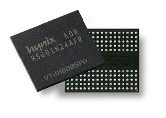
Hynix Semiconductor, Inc. has announced the second generation 1Gb (Gigabits) DDR3 using 54nm process technology. Hynix's new 1Gb DDR3, offered in x4 (H5TQ1G43TFR) and x8 (H5TQ1G83TFR) organizations, has innovative design modifications that significantly reduce power consumption of the device.

The new product operates at 1.5V (volts) power supply as the existing 1Gb DDR3 product and further reduces power consumption by 30% over the existing one. This second generation product is the highest performing memory in the industry among 1Gb density category which is the mainstream of the products. According to the iSuppli, a market research firm, the portion of the world wide 1Gb DDR3 is currently estimated to be 87%. The iSuppli estimates that higher densities will become the mainstream when it is expected to account for more than 50% in 2011.

Hynix Announces High Speed, Low Power 50nm-class DDR2 DRAM

Hynix Semiconductor, Inc. announced that it has developed the world's first mobile 1Gb DDR2 DRAM using 54nm process technology. By successfully developing a 50nm-class process, Hynix has overcome the challenge of producing mobile DRAMs with both high speed and low power consumption features.

This device is offered at a maximum speed of 1066MHz, and with 32-bit I/O, boasts bandwidth of 4.26GB/s(Giga byte per second) on a single channel device and 8.52GB/s on a dual channel. Hynix's 'One Chip Solution' design, offers the customer flexible options with 2-bit or 4-bit prefetch, and 16 or 32-bit I/O on a single chip. Additionally, Hynix's new mobile DDR2 is an eco-friendly device since it consumes only 50% of power compared to the previous generation mobile DDR, and 30% compared to standard DDR2 DRAM.

Hynix Semiconductor Develops the World’s First 2Gb Mobile DRAM

Hynix Semiconductor announced it has developed the world's first 2Gigabit mobile DRAM using 54nm process technology. This product provides twice as much storage capacity over current 1Gb mobile solution which has been the highest density offered among the mobile DRAM products in MCP(Multi Chip Package), PoP(Package on Package) platform. It boasts maximum operating speed of 400Mbps(Megabits per second) at 1.2V power supply and processes up to 1.6 Gigabytes of data per second with a 32-bit I/O. Moreover, the new product consumes less power than existing memory solutions.

Hynix Rolls-out 7 GT/s GDDR5 Memory Chip

DRAM major, Hynix has announced the depelopment of 7 GT/s GDDR5 memory chips for use by the visual-computing industry. These chips are built on the company's 54nm silicon fabrication technology.

The 1 Gb (128 MB) chips labelled H5GQ1H24AFR operate at the fastest speeds so far: 7 Gbps (or GT/s), which is a 40% boost in speeds compared to the older 5 GT/s chips already in production. The chip handles up to 28 GB of data per second across a 32-bit wide interface. The incorporation of new fab. processes also means reduced power consumption at 1.35V power supply. The JEDEC-standard 1Gb GDDR5 graphics DRAM chip targets high-end applications such as game consoles and graphics cards. The company will commence volume production in the first half of 2009.

Hynix to Produce 54nm DRAM Chips This Year

Hynix plans to produce 54nm-based DRAM chips this year on schedule, saying this will "reduce the technology gap with Samsung," according to the company's CEO, quoted by the Korea Times. The company schedules to start production of 54-nano DRAMs in the third quarter, while Samsung is expected to commence production of 56-nano DRAMs near the end of the second quarter. The company also plans to gradually increase its use of 300mm chip fabrication lines to account for 95 percent of its entire DRAM production by 2012. The company runs three 300mm lines and five 200mm lines in its two plants in South Korea and one in China.
Return to Keyword Browsing
Sep 17th, 2024 10:22 EDT change timezone

New Forum Posts

Popular Reviews

Controversial News Posts