News Posts matching #Arizona

Return to Keyword Browsing

TSMC Fast-Tracks US Fabs, Europe and Japan Fall Behind

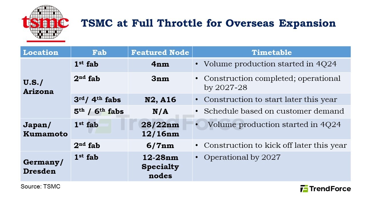
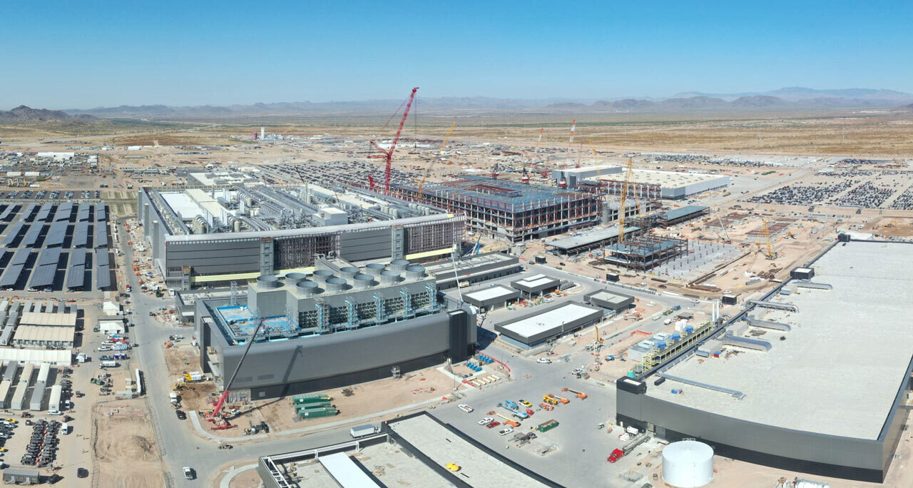
TSMC is adjusting its global investment strategy in response to geopolitical pressures and changing market demands. Encouraged by the US government, the world's largest contract chipmaker has moved up completion dates for its Arizona fabrication plants by as much as six months. This shift is designed to address the growing domestic needs in defense, artificial intelligence, and high-performance computing. Originally committed to $65 billion in US manufacturing, TSMC recently increased that total to $165 billion. The expanded plan includes three additional fabs, two advanced packaging facilities, and a research center, all of which are expected to begin operation by 2030. Company executives argue that on-site production will help alleviate supply-chain bottlenecks and reduce cost volatility for American customers, even though chips made in Arizona will carry a premium compared with those produced in Taiwan.

At the same time, TSMC's projects in Japan and Germany have encountered difficulties. In Kumamoto, Fab 1 has not reached its planned utilization levels, and persistent traffic and local infrastructure issues have delayed the start of construction for Fab 2. Some point to labor shortages and conservative order forecasts from automotive and electronics clients as additional factors. In Europe, a slowdown in auto production has weakened demand for semiconductor capacity. TSMC's joint venture with Bosch, Infineon, and NXP in Germany now faces potential delays as partner layoffs and declining sales of combustion engines undermine initial growth expectations. Despite these setbacks, Taiwan remains central to TSMC's operations, hosting nearly half of its nine facilities under construction. For now, TSMC's pause in Japan and Europe appears to be a strategic reallocation of resources to the US, where policy support and urgent demand intersect.

TSMC Reportedly Surpasses 90% Production Yield Rate with 2 nm Process

At the tail end of Q1'25, industry whispers suggested that TSMC's premier facilities had completed cutting/leading-edge 2 nm (N2) trial production runs. By early April, company insiders alluded to a confident push into preparations for a futuristic 1.4 nm node at the "P2" Baoshan Plant. This is a very distant prospect; watchdogs envision a 2028 release window. According to expert predictions, cross-facility 2 nm wafer mass production phases are expected to start by the end of this year. Foundry staff seem to be actively pursuing an improvement in yields; earlier guesstimates indicated the crossing of a 70% milestone—good enough for full-blown manufacturing runs.

Fresher musings point to staffers and advanced equipment achieving and stepping just beyond an impressive 90% mark, albeit with silicon intended for "memory products." As of mid-May, Samsung's competing "SF2" product—allegedly—remains in testing phases. South Korean insider news reports posit 2 nm GAA trial yields passing 40%—a significant development for the megacorp's foundry business. Roughly a month ago, (in public) TSMC leadership spoke about an unprecedented demand for 2 nm wafers. Due to rumors of greater than anticipated charges for important TSMC clients, Samsung Semi's top brass is supposedly trying to woo the likes of NVIDIA and Qualcomm.

AMD Reportedly Shifts from Samsung to TSMC's 4nm Arizona Facility

AMD has reportedly decided to move its 4 nm chip orders from Samsung to TSMC's facilities in Arizona, United States. This is a significant loss for Samsung, as AMD had been working closely with Samsung on the SF4X process for EPYC server processors, Ryzen APUs, and Radeon graphics cards. It's worth noting that in May 2023, AMD announced the exact opposite—moving from TSMC to Samsung for some of its 4 nm CPUs. This partnership was an important part of AMD's strategy to use multiple manufacturers; however now appears to be failing. Reports indicate that AMD's decision comes from concerns about the stability and consistency of Samsung's manufacturing process, leading AMD to cancel plans for mass production of graphics chips using Samsung's 4 nm technology.

These changes in manufacturing strengthen TSMC's leading position in the chip manufacturing industry, even though relying on a single manufacturer creates geopolitical risks. AMD continues to deepen its relationship with TSMC, committing to use TSMC's advanced 2 nm technology for its upcoming "Venice" processors, which have completed testing at TSMC's Arizona facility and remain on schedule for release in 2026. Meanwhile, Samsung Electronics has reportedly achieved better-than-expected results in testing its SF2 (2 nm) process, with initial yields above 30%. The company plans to stabilize this process in the second half of 2025 to begin mass production of the Exynos 2600 mobile chip. Building on this progress, Samsung is reportedly close to securing an agreement to manufacture Qualcomm's Snapdragon 8 Elite 2 using its new 2 nm process.

TSMC Reportedly Begins Construction of Third Arizona Production Location

As disclosed in a new press release—issued by the US Commerce Department—TSMC's North American operation has started another expansion. Last month, Taiwan's leading chip foundry committed a substantial $100 billion investment—eventually leading to a greater production footprint in Phoenix, Arizona. Reports suggest that ground has already been broken, in a low-key manner—as of yesterday (April 29)—at a planned third location, only hours after TSMC's receiving of permits—aka a "thumbs up" from the US government. According to local news outlets, key administrative representatives were in attendance to witness the initiation of construction work. TSMC's third plant is destined to pump out cutting-edge products via a 2 nm (N2) process technology, with Apple, NVIDIA and AMD confirmed as "front of the queue" customers. Despite recent fanfare and celebrations, industry analysts reckon that it will take up to a decade for the foundry's North American operation to solidify a dependable supply chain. In the interim, certain elements will require shipping to overseas locations—for packaging and finalization purposes.

TSMC's US Supply Chain to Take Up To a Decade to Complete

According to reports in the Taiwan media, TSMC's suppliers have stated that they are willing to accompany TSMC on its expansion in the US. This comes on the back of TSMC's pledge in March to invest US$100 billion in Arizona where its current fabs are located. However, due to TSMC's currently limited production quantities in the US there's little incentive for these companies to set up branch offices in the US, even taking the tariffs into account. In other words, it might take up to a decade before TSMC has a comparable supply chain in the US, to that it has in Taiwan and China today.

The Taiwan government has discussed the matter with various chemical suppliers and the conclusion was that TSMC's production volumes at the moment don't warrant the costs of setting up a local supply chain and that it's likely to take seven to eight years for them to be fully established in the US from the get-go. On the other hand, if TSMC's volumes reach the proposed levels that the company has outlined in its fab roadmaps, we're likely to see most of its supply chain partners setting up business in the US. This also suggests that TSMC might not have bothered with approaching Intel's suppliers, which is somewhat surprising, as many of them ought to be able to provide similar chemicals and materials as TSMC's suppliers in Taiwan offer the company. It's also possible that Intel's suppliers haven't provided pricing that TSMC finds competitive enough. Regardless, at some point in the future, there's likely to be more competition when it comes to semiconductor production materials suppliers, assuming TSMC expands its fabs according to plan.

TSMC Expects to Produce 30 Percent of its Sub-2nm Chips in the US, Denies Intel Joint Venture

On the back of TSMC's first quarter report, news is coming out of Taiwan that the company is expecting to produce as much as a third of its sub 2 nm chips in its US fabs, at some point in the future. This is according to comments made by TSMC's chair and CEO C.C. Wei during its online investors conference. As we've already mentioned, TSMC is looking to expand in Arizona with a further two fabs later this year, both targeting sub 2 nm chip production, but the comments by the CEO suggests that these might be bigger fabs than initially expected, if they're going to be able to produce as much as a third of all of TSMC's sub 2 nm output by some time around the next decade.

Apparently the move to build the new fabs is due to increased demand from TSMC's US customers, which includes AMD, Apple, NVIDIA, Qualcomm and Broadcom, to mention its biggest US customers. It seems like those that are planning to produce chips at TSMC's new fabs in the US are accepting an increase in cost, although it has apparently been framed as a value proposition from TSMC's side towards its customers, which have accepted it as such. At the same time Wei once again refuted that TSMC is in any kind of talks with Intel or any other companies about joint ventures, technology licensing or technology transfer. This should put further rumours about any form of joint venture to rest for now.

TSMC Expands U.S. Footprint with Two New Fabs in Arizona

TSMC is speeding up its plans to grow worldwide, the company's Chairman, C.C. Wei is announcing they'll start building their third and fourth fabs in Arizona later this year. This comes after TSMC finished constructing the second Arizona plant while the first fab started volume production in Q4 2024. TSMC wants to open its second factory about six months earlier than planned due to increasing customer demand. The first factory will make 4 nm chips, the second will target 3 nm chips, and the newer ones will work on even smaller N2 and A16 nodes. This rapid expansion is part of TSMC's additional $100 billion investment to build five more semiconductor plants and a research center in the U.S. In total, TSMC will invest $165 billion in the United States.

Besides its US operations, TSMC keeps pushing forward with its worldwide manufacturing plans. Wei dismissed rumors of setbacks at the company's upcoming Kumamoto plant in Japan. He confirmed that their first fab started mass production in late 2024, achieving excellent yields. They plan to begin building a second Japanese facility this year, once the infrastructure is ready. The company's European expansion in Dresden is also on track, with strong backing from both the European Commission and the German federal government. They broke ground at the Dresden site in August 2024 as Europe's first FinFET-capable dedicated foundry operation.

NVIDIA & Partners to Produce American-made AI Supercomputers in US for First Time

NVIDIA is working with its manufacturing partners to design and build factories that, for the first time, will produce NVIDIA AI supercomputers entirely in the U.S. Together with leading manufacturing partners, the company has commissioned more than a million square feet of manufacturing space to build and test NVIDIA Blackwell chips in Arizona and AI supercomputers in Texas. NVIDIA Blackwell chips have started production at TSMC's chip plants in Phoenix, Arizona. NVIDIA is building supercomputer manufacturing plants in Texas, with Foxconn in Houston and with Wistron in Dallas. Mass production at both plants is expected to ramp up in the next 12-15 months. The AI chip and supercomputer supply chain is complex and demands the most advanced manufacturing, packaging, assembly and test technologies. NVIDIA is partnering with Amkor and SPIL for packaging and testing operations in Arizona.

Within the next four years, NVIDIA plans to produce up to half a trillion dollars of AI infrastructure in the United States through partnerships with TSMC, Foxconn, Wistron, Amkor and SPIL. These world-leading companies are deepening their partnership with NVIDIA, growing their businesses while expanding their global footprint and hardening supply chain resilience. NVIDIA AI supercomputers are the engines of a new type of data center created for the sole purpose of processing artificial intelligence—AI factories that are the infrastructure powering a new AI industry. Tens of "gigawatt AI factories" are expected to be built in the coming years. Manufacturing NVIDIA AI chips and supercomputers for American AI factories is expected to create hundreds of thousands of jobs and drive trillions of dollars in economic security over the coming decades.

TSMC Accelerates US "Fab 21" Expansion Following Early Setbacks

TSMC is reconfiguring its US strategy after a challenging start at its Fab 21 facility near Phoenix, Arizona. The company's initial module took nearly five years to move from groundbreaking to production—far longer than the typical two-year process observed in Taiwan. Early setbacks, including labor issues, rising costs, and cultural differences, slowed progress, but these hurdles have provided valuable lessons. With a clearer understanding of the local construction environment, TSMC plans to speed up future projects. Company executives have identified reliable local contractors and addressed many bottlenecks that once hindered progress. As a result, the Taiwanese maker is gearing up to accelerate construction timelines for its upcoming modules. Notably, TSMC intends to start building its third fab—Fab 21 module 3—this year, aiming for a pace similar to that in Taiwan.

In the current phase, TSMC is finalizing equipment installations for Fab 21 module 1 while laying the groundwork for module 2. The plan is to begin trial production of advanced 3 nm-class chips at module 2 in 2026, with high-volume manufacturing expected to kick off by 2028. The accelerated schedule for module 3 is seen as a pathway to faster production of next-generation chips, including those using the N2-series and A16 process technologies. However, rapid construction is not without risks. A critical concern remains the timely procurement of essential fab tools. Leading suppliers such as ASML and Applied Materials face significant backlogs and capacity constraints, which may delay the delivery of necessary equipment. As TSMC vows to build its US capacity more swiftly, the entire supply chain is watching closely to see if these supply chain challenges can be resolved, ensuring that the company meets its ambitious production timelines while expanding its foothold in the American market.

TSMC Arizona Operations Only 10% More Expensive Than Taiwanese Fab Operations

A recent study by TechInsights is reshaping the narrative around the cost of semiconductor manufacturing in the United States. According to the survey, processing a 300 mm wafer at TSMC's Fab 21 in Phoenix, Arizona, is only about 10% more expensive than similar operations in Taiwan. This insight challenges earlier assumptions based on TSMC founder Morris Chang's comments, which suggested that high fab-building expenses in Arizona made US chip production financially impractical. G. Dan Hutcheson of TechInsights highlighted that the observed cost difference largely reflects the expenses associated with establishing a brand-new facility. "It costs TSMC less than 10% more to process a 300 mm wafer in Arizona than the same wafer made in Taiwan," he explained. The initial higher costs stem from constructing a fab in an unfamiliar market with a new, sometimes unskilled workforce—a scenario not typical for mature manufacturing sites.

A significant portion of the wafer production cost is driven by equipment, which accounts for well over two-thirds of the total expenses. Leading equipment providers like ASML, Applied Materials, and Lam Research charge similar prices globally, effectively neutralizing geographic disparities. Although US labor costs are higher than in Taiwan, the heavy automation in modern fabs means that labor represents less than 2% of the overall cost. Additional logistics for Fab 21, including the return of wafers to Taiwan for dicing, testing, and packaging, add complexity but only minimally affect the overall expense. With plans to expand domestic packaging capabilities, TSMC's approach is proving to be strategically sound. This fresh perspective suggests that the apparent high cost of US fab construction has been exaggerated. TSMC's $100B investment in American semiconductor manufacturing reflects a calculated decision informed by detailed cost analysis—demonstrating that location-based differences become less significant when the equipment dominates expenses.

NVIDIA Plans US Supply Chain Investment Worth Hundreds of Billions, "Blackwell" Already Manufactured in Arizona

NVIDIA's CEO Jensen Huang made some interesting commentary for the Financial Times, stating that the company will procure over half a trillion US Dollars worth of electronics over the next four years, and it it plans to keep hundreds of billions from the supply chain procurement in the US. "Overall, we will procure, over the course of the next four years, probably half a trillion dollars worth of electronics in total. And I think we can easily see ourselves manufacturing several hundred billion of it here in the US," said Jensen for FT. NVIDIA currently manufactures its silicon at TSMC's facilities, as well as electronics like motherboards and servers at Foxconn. However, the geopolitical situation is making NVIDIA reconsider its supply chain dependencies, and the company is looking for more US-based manufacturing.

NVIDIA confirmed that its latest "Blackwell" series of GPUs, including the latest Blackwell Ultra, are being manufactured at TSMC's Arizona facilities. TSMC announced a $100 billion investment in its Arizona expansion, and NVIDIA is ready to take up more of TSMC's capacity to meet its ever-growing demand for GPUs. During the GTC 2025 event, Jensen noted that only four cloud service providers will use 3.6 million GPUs this year. That is without any AI labs and enterprises, which are massive consumers of GPUs (xAI only has 200,000 GPU clusters). To continue manufacturing excellence so customers won't suffer, NVIDIA is also looking at other options for supply chain manufacturing partners. Intel, the only US-based company capable of producing advanced silicon, is a potential target for NVIDIA. "We evaluate their foundry technology on a regular basis, and we are ongoing in doing that... We look for opportunities to be a customer of theirs... I have every confidence that Intel can do it," added Jensen, who also stated that NVIDIA is interested in silicon manufacturing and chip packaging services, as Intel's Foveros 3D packaging and other technologies are attractive for Team Green.

Intel Announces Ohio One Construction Timeline Update

On Feb. 28, 2025, Naga Chandrasekaran, executive vice president, chief global operations officer and general manager of Intel Foundry Manufacturing, sent a message to Intel employees in Ohio updating them on the latest planned construction completion dates for Ohio One Mod 1 and Mod 2 that are under construction in New Albany, Licking County, Ohio. I continue to be impressed by the progress you are driving on our Ohio One campus. We have come a long way since construction began, and I am grateful for all that you've accomplished to lay the groundwork for our future as we make Ohio one of the world's leading hubs of advanced semiconductor manufacturing.

Last quarter, we achieved our "go vertical" milestone when the "basement" level of the fab was completed - and work on the above-ground structure is now underway. The campus has been transformed in ways that bring Ohio's natural beauty to the site. You are also doing so much beyond our campus to support Ohioans in our neighborhood and across the state by creating education and workforce development initiatives, building local business partnerships, and volunteering and investing in the community. I am proud of the impact you are making.

TSMC CEO Believes American Foundries Will Trail Behind Primary Taiwanese Sites

C.C. Wei, TSMC CEO and Chairman, has shared his latest views regarding his company's North American manufacturing center—Reuters cornered him for comment during a mid-week appearance at a National Taiwan University-held event. The Taiwanese government has recently lowered its "silicon shield"—following much (reported) deliberation over "legal restrictions on transferring leading-edge process technology overseas." This relaxation of rules has TSMC considering a new set of investments for operations outside of Taiwan—with an expansion into advanced node process manufacturing. Currently, 2 nm (N2) is a home turf-speciality—industry experts estimate an expenditure of $28-30 (USD) billion to bring this production technology over to the States. TSMC's CEO has described additional challenges—on top of (and impacting) finances—local bureaucracy is a big one.

Wei stated: "every step requires a permit, and after the permit is approved, it takes at least twice as long as in Taiwan." According Reuters, he reckons that it would be difficult for their North American sites to access the latest technologies ahead of teams in Taiwan. He detailed his company's recruitment of several experts—tasked with talking to local government; about regulatory issues. This was not a cheap undertaking: "we ended up establishing 18,000 rules, which cost us $35 million." TSMC's Arizona production hub will (eventually) consist of three large factories—despite long-term teething problems, Fab 21 is reported to be churning out the first wave of "Made in America" product for a very important client: Apple. Wei expressed positives views when asked about the USA site's prospects—during an earnings conference (Jan 16)—he believes that it will eventually produce the "same quality of chips as in Taiwan," through a "smooth ramp-up process."

Apple Reportedly Due to Receive First Batch of "Made in USA" TSMC Chips

The latest news reports suggest that Apple is currently verifying the quality of TSMC Arizona-made chips—the process has reached a "final test stage" with samples from an initial batch being compared to "Made in Taiwan" product. TSMC's native foundries—utilizing the latest cutting-edge technologies—are accustomed to pumping out plenty of high-quality and advanced chips. Nikkei Asia believes that an approval—if USA-made silicon passes muster—will result in commercial mass-produced chips being delivered as soon as Q1 2025. This would be a significant victory for TSMC's relatively new Arizona fab—reported teething problems have caused delays and budgets to balloon. Apple could be the first of TSMC's customers to send products to market that have Arizona-manufactured silicon onboard.

Taiwan's chip-making industry is facing an uncertain future due to regional political tensions—in reaction, the nation's government has started shifting its stance on guarding TSMC's most advanced production processes. Leading-edge process technologies could be heading overseas, with new investments being considered at the Arizona campus. TSMC and Amkor are working on setting up advanced packaging and test facilities at the Peoria location, so current logistics are not ideal—US-made product has to be sent to an Amkor packaging facility in Taiwan. TSMC USA's future looks quite promising—AMD and NVIDIA are reportedly the next in line to receive locally produced samples for verification. Industry moles reckon that Team Green's advanced "Blackwell" AI GPUs could be produced in Peoria—based on alleged partnership negotiations from late last year.

TSMC Arizona Plant Operations Will Reportedly Cost 30% More Than Taiwan Sites

TSMC's new semiconductor manufacturing facility in Phoenix, Arizona, will face production costs approximately 30% higher than its Taiwan-based operations when it begins mass production in early 2025. The increased expenses stem from higher tariffs and transportation costs associated with importing necessary materials from Taiwan. The Arizona facility will start producing 10,000 12-inch wafers monthly using a 4 nm node, with plans to double output to 20,000 wafers at full capacity. Four major technology companies—Apple, NVIDIA, AMD, and Qualcomm—have committed to purchasing chips from the plant for their AI and high-performance computing needs. The 445-hectare facility highlights ongoing challenges in America's semiconductor industry. Despite the aim to strengthen domestic chip manufacturing, the plant must import materials from Taiwan to maintain production quality, revealing gaps in the US semiconductor supply chain.

This overseas dependency drives up operational costs significantly. While TSMC's investment marks an essential step in rebuilding domestic capacity, the substantial cost difference between US and Taiwanese production raises questions about long-term viability. TSMC has already begun trial production at the site and plans to expand operations with additional phases. The company's Phase 2 facility is completed, and equipment is being installed, while future expansions aim to produce 2 nm chips by 2028. However, unless the cost gap narrows, the higher production expenses could impact the plant's competitiveness in the global semiconductor market, even competing with its own Taiwanese facilities, where customers could decide to use Taiwanese fabs due to lower costs. Meanwhile, TSMC continues to expand its Taiwan operations, with plans to build new 2 nm facilities in Kaohsiung's Science Park starting next year.

TSMC and NVIDIA Reportedly in Talks to Bring "Blackwell" GPU Production to Arizona

TSMC is reportedly negotiating with NVIDIA to manufacture advanced "Blackwell" GPUs in its Arizona facility. First reported by Reuters, this partnership could mark another major shift in AI chip production toward US soil. The discussion centers around TSMC's Fab 21 in Phoenix, Arizona, specializing in 4 nm and 5 nm chip production. NVIDIA's Blackwell GPUs utilize TSMC's 4NP process technology, making the Arizona facility a technically viable production site. However, the proposed arrangement faces several logistical challenges. A key issue is the absence of advanced packaging facilities in the United States. There is Amkor that planned to do advanced packaging, but it's only scheduled to begin packaging in 2027. TSMC's sophisticated CoWoS packaging technology is currently available only in Taiwan. This means that chips manufactured in Arizona would need to be shipped back to Taiwan for final assembly, potentially increasing production costs.

While alternative solutions exist, such as redesigning the chips to use Intel's packaging technology or focusing on gaming GPU production in Arizona, these options present their own complications. Intel's packaging methods would likely increase costs, and the current absence of graphics card manufacturing infrastructure in the US makes domestic gaming GPU production less practical. Both TSMC and NVIDIA have declined to comment on the ongoing negotiations, as this is confidential information unknown to the public. Interestingly, TSMC's Arizona facility has already attracted a few more US firms for domestic manufacturing, like Apple, rumored to manufacture its A16 Bionic chip and AMD with high-performance designs, likely either EPYC or Instinct MI chips.

TSMC Delays Arizona Facility "Fab 21" Opening to January 2025

TSMC has reportedly postponed the opening ceremony of its Arizona Fab 21 facility, initially planned for December 6, amidst the changing US political landscape. The ceremony is now expected to take place after President-elect Donald Trump's inauguration in early 2025, showing that the chipmaker is taking a cautious approach to geopolitical shifts. The delay comes as TSMC finds itself at the intersection of global semiconductor politics. The company has invested heavily in its Arizona operations (estimated at $65 billion total), with Wang Yinglang, deputy general manager of wafer factory operations, leading the project. Despite initial skepticism, Wang's team has maintained an ambitious timeline, with mass production scheduled to begin in the first half of 2025.

Rumors also suggest that TSMC's decision stems from broader concerns about the incoming administration's semiconductor policies. However, TSMC maintains a strong position due to its unmatched technological capabilities, particularly in advanced manufacturing processes, which competitors like Intel and Samsung struggled to achieve. The Arizona facility represents a crucial piece of TSMC's global expansion strategy, which includes new factories in Japan and Germany. While the company faces challenges, including labor issues and rising costs in the US, its strategic importance to the global semiconductor supply chain remains unchanged. The only thing that is changing is the timeline of the opening ceremony, while high-volume production stays on track.

TSMC Can't Legally Make 2 nm Chips in the US Yet, Latest Nodes Must Remain in Taiwan

Even with billions of US dollars being invested overseas, TSMC cannot legally manufacture its most advanced nodes outside of Taiwan. According to Taiwan's Minister of Economic Affairs J.W. Kuo, "Since Taiwan has regulations to protect its own technologies, TSMC cannot produce 2-nanometer chips overseas currently." He added, "Although TSMC plans to make 2-nanometer chips [abroad] in the future, its core technology will stay in Taiwan." This provides crucial insight into TSMC's strategic positioning, both in its US expansion plans and in navigating global geopolitical waters, especially with Taiwan being the major hub of silicon innovation. Taiwan's semiconductor industry follows strict regulations regarding overseas production capabilities, requiring companies to maintain their most advanced manufacturing processes within Taiwan.

The company's international expansion strategy includes significant developments in the United States. TSMC's Arizona facilities are central to these plans, with multiple fabs in different stages of development. The initial Arizona facility will begin producing 4 nm chips imminently, while a second facility, scheduled to open in 2028, will manufacture then mature 3 nm and 2 nm chips. A third planned facility aims to produce 2 nm or more sophisticated chips. Meanwhile, Taiwan-based facilities will produce more advanced chips at the same time, with volume production of A-16 chips planned for late 2026, following the rollout of 2 nm chip production in 2025. Furthermore, Taiwan-US semiconductor cooperation will continue regardless of political changes. Taiwan Semiconductor Industry Association (TSIA) Chairman and TSMC Senior Vice President Cliff Hou noted that historical evidence suggests US electoral outcomes have not significantly impacted this technological partnership, though some adjustments may occur.

TSMC Arizona Achieves 4% Higher Yields Than Taiwanese Facilities, Marking Progress for US Silicon Manufacturing

The American semiconductor landscape reached a significant milestone as TSMC's new Arizona manufacturing facility demonstrated remarkable production efficiency, exceeding its Taiwanese counterparts by 4% in yield rates. This achievement, revealed at a recent industry webinar by the company's US division chief, represents a major step forward in America's push to strengthen domestic chip manufacturing capabilities. Since initiating its 4 nm node production operations this spring, the Phoenix-based facility has demonstrated impressive technical proficiency, achieving production standards that match and surpass TSMC's established Taiwanese facilities. The project, backed by substantial federal support, including $11.6 billion in combined grants and loans plus significant tax incentives, aims to establish three cutting-edge manufacturing plants in Arizona.

The company's global leadership praised the facility's performance, noting its strategic importance in demonstrating TSMC's ability to maintain exceptional manufacturing standards across international locations. This success carries particular weight given the project's earlier hurdles, which included workforce challenges and timeline adjustments that shifted the entire production schedule by approximately one year. This development gains additional significance against industry-wide challenges, particularly as competitors like Intel and Samsung face operational and financial obstacles. The semiconductor giant's plans now extend to potential further expansion, with the Phoenix site capable of hosting up to six manufacturing facilities. Future growth prospects could be enhanced by proposed additional government initiatives supporting domestic chip production.

AMD to Become Major Customer of TSMC Arizona Facility with High-Performance Designs

After Apple, we just learned that AMD is the next company in line for US-based manufacturing in the TSMC Arizona facility. Industry analyst Tim Culpan reports that TSMC's Fab 21 in Arizona will soon be producing AMD's high-performance computing (HPC) processors, with tape out and manufacturing expected to commence on TSMC's 5 nm node next year. This move comes after previously reported Apple's A16 SoC production, which is already in progress at the facility and could see shipments before the end of this year, significantly ahead of the initially projected early 2025 schedule. The production of AMD's HPC chips in Arizona marks a crucial step towards establishing an AI-hardware supply chain operating entirely on American soil, which is expected to further expand with Intel Foundry and Samsung Texas facility.

Making HPC processors domestically serves as a significant milestone in reducing dependence on overseas semiconductor manufacturing and strengthening the US's position in the global chip industry. Adding to the momentum, TSMC and Amkor recently announced a collaboration on advanced packaging technologies, including Integrated Fan-Out (InFO) and Chip-on-Wafer-on-Substrate (CoWoS), which are vital for high-performance AI chips. However, as Amkor facilities are yet to be built, these chips are going to be shipped back to Taiwan for packaging before being integrated into the final product. Once the Amkor facility is up and running, Arizona will become the birthplace of fully manufactured and packaged silicon chips.

Amkor and TSMC to Expand Partnership and Collaborate on Advanced Packaging in Arizona

Amkor Technology, Inc. and TSMC announced today that the two companies have signed a memorandum of understanding to collaborate and bring advanced packaging and test capabilities to Arizona, further expanding the region's semiconductor ecosystem.

Amkor and TSMC have been closely collaborating to deliver high volume, leading-edge technologies for advanced packaging and testing of semiconductors to support critical markets such as high-performance computing and communications. Under the agreement, TSMC will contract turnkey advanced packaging and test services from Amkor in their planned facility in Peoria, Arizona. TSMC will leverage these services to support its customers, particularly those using TSMC's advanced wafer fabrication facilities in Phoenix. The close collaboration and proximity of TSMC's front-end fab and Amkor's back-end facility will accelerate overall product cycle times.

TSMC Produces Apple A16 Chips in Arizona Facility, a First on the American Soil

TSMC has reportedly initiated production of Apple's last-generation A16 Bionic processors at its newly constructed Fab 21 in Arizona. This development comes significantly earlier than anticipated, with the facility's full-scale production initially scheduled for 2025. According to insights from industry expert Tim Culpan, the Arizona plant is already churning out a modest but noteworthy quantity of A16 Bionic chips. These processors are being manufactured using TSMC's NP4 4 nm semiconductor node. Culpan also hinted at a substantial increase in production capacity once the second stage of Fab 21's initial phase becomes operational.

This early start serves a critical function for TSMC, allowing the company to calibrate its advanced equipment and refine its manufacturing processes thoroughly. Using the well-established A16 Bionic design, TSMC can ensure its new facility meets the exacting standards required for next-generation semiconductor production. The news aligns with recent industry buzz suggesting that Fab 21 is already achieving yield rates comparable to TSMC's long-established Taiwanese plants—a remarkable feat for a newly launched facility. While current output remains limited, this milestone marks a significant step in TSMC's expansion into US-based chip manufacturing. With more fabs on American soil, companies can push domestic manufacturing and ensure that geopolitics don't hinder the vital supply chain.

TSMC Arizona Achieves Yield Parity with Taiwanese Facilities, Production Remains on Schedule

TSMC has reportedly managed to produce yields at its Arizona facility that are on par with yields back home in Taiwan, making its expansion efforts successful. According to Bloomberg, TSMC did a trial production, a multi-month effort, to produce N4 node wafers with low defect rates. With wafers now in TSMC's labs for testing, it is reported that Arizona facility yields have achieved parity with their Taiwanese facilities back home. This indicates that TSMC's efforts to expand in the US are so far considered a success, as advanced chipmaking is a very complex process that is only done by a few makers and in very few locations. With TSMC expanding in the US now and proving that its technology can work on US soil, the company has a green light to start volume production in the first half of 2025.

However, this is only the beginning of TSMC's Arizona expansion. The Taiwanese giant plans to have a second fab operational by 2028 and produce 2 nm and 3 nm chips in the state. Additionally, there will be a third facility for 2 nm and more advanced nodes in Phoenix, bringing the total value of TSMC's US expansion efforts to $65 billion, with $6.6 billion from the CHIPS Act grants and $5 billion in loans from the US government. If upcoming fabs follow the lead of the first facility, US-based production needs will possibly be satisfied.

TSMC to Introduce Location Premium for Overseas Chip Production

As a part of its Q1 earnings call discussion, one of the largest semiconductor manufacturers, TSMC, has unveiled a strategic move to charge a premium for chips manufactured at its newly established overseas fabrication plants. During an earnings call, TSMC's CEO, C.C. Wei, announced that the company will impose higher pricing for chips produced outside Taiwan to offset the higher operational costs associated with these international locations. This move aims to maintain TSMC's target gross margin of 53% amidst rising expenses such as inflation and elevated electricity costs. This decision comes as TSMC expands its global footprint with new facilities in the United States, Germany, and Japan (JAMS) to meet the increasing demand for semiconductor chips worldwide. The company's new US-based Arizona facility, known as Fab 21, has faced delays due to equipment installation issues and labor negotiations.

Chips produced at this site, utilizing TSMC's advanced N5 and N4 nodes, could cost between 20% to 30% more than those manufactured in Taiwan. TSMC's strategy to manage the cost disparities across different geographic locations involves strategic pricing, securing government support, and leveraging its manufacturing technology leadership. This approach reflects the company's commitment to maintaining its competitive edge while navigating the complexities of global semiconductor manufacturing in today's fragmented market. Introducing a location premium is expected to impact American semiconductor designers, who may need to pass these costs on to specific market segments, particularly those with lower price sensitivity, such as government-related projects. Despite these challenges, TSMC's overseas expansion underscores its adaptive strategies in the face of global economic pressures and industry demands, ensuring its continued position as a leading player in the semiconductor industry.

Arizona State University and Deca Technologies to Pioneer North America's First R&D Center for Advanced Fan-Out Wafer-Level Packaging

Arizona State University (ASU) and Deca Technologies (Deca), a premier provider of advanced wafer- and panel-level packaging technology, today announced a groundbreaking collaboration to create North America's first fan-out wafer-level packaging (FOWLP) research and development center.

The new Center for Advanced Wafer-Level Packaging Applications and Development is set to catalyze innovation in the United States, expanding domestic semiconductor manufacturing capabilities and driving advancements in cutting-edge fields such as artificial intelligence, machine learning, automotive electronics and high-performance computing.
Return to Keyword Browsing
Jul 5th, 2025 17:55 CDT change timezone

New Forum Posts

Popular Reviews

TPU on YouTube

Controversial News Posts