News Posts matching #Chiplet

Return to Keyword Browsing

Winbond Joins UCIe Consortium to Support High-performance Chiplet Interface Standardisation

Winbond has joined the UCIe (Universal Chiplet Interconnect Express) Consortium, the industry Consortium dedicated to advancing UCIe technology. This open industry standard defines interconnect between chiplets within a package, enabling an open chiplet ecosystem and facilitating the development of advanced 2.5D/3D devices.

A leader in high-performance memory ICs, Winbond is an established supplier of known good die (KGD) needed to assure end-of-line yield in 2.5D/3D assembly. 2.5D/3D multichip devices are needed to realize the exponential improvements in performance, power efficiency, and miniaturization, demanded by the explosion of technologies such as 5G, Automotive, and Artificial Intelligence (AI).

Open Compute Project Foundation and JEDEC Announce a New Collaboration

Today, the Open Compute Project Foundation (OCP), the nonprofit organization bringing hyperscale innovations to all, and JEDEC Solid State Technology Association, the global leader in the development of standards for the microelectronics industry, announce a new collaboration to establish a framework for the transfer of technology captured in an OCP-approved specification to JEDEC for inclusion in one of its standards. This alliance brings together members from both the OCP and JEDEC communities to share efforts in developing and maintaining global standards needed to advance the electronics industry.

Under this new alliance, the current effort will be to provide a mechanism to standardize Chiplet part descriptions leveraging OCP Chiplet Data Extensible Markup Language (CDXML) specification to become part of JEDEC JEP30: Part Model Guidelines for use with today's EDA tools. With this updated JEDEC standard, expected to be published in 2023, Chiplet builders will be able to provide electronically a standardized Chiplet part description to their customers paving the way for automating System in Package (SiP) design and build using Chiplets. The description will include information needed by SiP builders such as Chiplet thermal properties, physical and mechanical requirements, behavior specifications, power and signal integrity properties, testing the Chiplet in package, and security parameters.

Chinese Loongson Processor Uses Chiplet Design to Pack 32 Cores

Chinese processor designers need help creating a leading-edge design that satisfies their needs, with the imposed sanctions and restrictions of Western countries. However, designers are using creative ways to make a server processor to fulfill their needs. According to the latest Sina report, Chinese company Loongson has developed a 32-core processor using chiplet technology. Previously, the company announced its 16-core 3C5000 processor based on LA464 cores, which utilize LoongArch ISA. Loongson used chiplet technology to fuse two 3C5000 processors into a single-socket solution called 3D5000, which features 32 LA464 cores to create a higher-performing design. Based on the LGA-4129 package, the chip size is 75.4x58.5×6.5 mm.

The company claims that the typical power consumption is rated for 130 Watts at 2.0 GHz or 170 Watts at 2.2 GHz, with TDP power consumption not exceeding 300 Watts at 2.2 GHz even with peaks. The performance of the new 3D5000 processor, measured using SPEC2006, is 400 points and 800 points for single-socket and dual-socket servers, respectively. The four-socket server is expected to reach 1600 points in the same benchmark, so scaling is advertised as linear. Loongson hopes to provide samples to industry partners in the first half of 2023 with an unknown price tag.

Ventana Introduces Veyron, World's First Data Center Class RISC-V CPU Product Family

Ventana Micro Systems Inc. today announced its Veyron family of high performance RISC-V processors. The Veyron V1 is the first member of the family, and the highest performance RISC-V processor available today. It will be offered in the form of high performance chiplets and IP. Ventana Founder and CEO Balaji Baktha will make the public announcement during his RISC-V Summit keynote today.

The Veyron V1 is the first RISC-V processor to provide single thread performance that is competitive with the latest incumbent processors for Data Center, Automotive, 5G, AI, and Client applications. The Veyron V1 efficient microarchitecture also enables the highest single socket performance among competing architectures.

AMD Still Believes in Moore's Law, Unlike NVIDIA

Back in September, NVIDIA's Jensen Huang said that Moore's Law is dead, but it seems like AMD disagrees with NVIDIA, at least for now. According to an interview with AMD's CTO, Mark Papermaster, AMD still believes that Moore's Law will be alive for another six to eight years. However, AMD no longer believes that transistor density can be doubled every 18 to 24 months, while remaining in the same cost envelope. "I can see exciting new transistor technology for the next - as far as you can really plot these things out - about six to eight years, and it's very, very clear to me the advances that we're going to make to keep improving the transistor technology, but they're more expensive," Papermaster said.

AMD believes we'll see a change in how chips are being designed and put together, with chiplets being the future of semiconductors. Papermaster calls this "a Moore's Law equivalent, meaning that you continue to really double that capability every 18 to 24 months" although it's not exactly Moore's Law in the traditional sense. AMD also appears to be betting heavily on FPGA technology in some of its market segments, for something the company calls adaptive computing. As to how things will play out, time will tell, but with both AMD and Intel going down the chiplet route, albeit in slightly different ways, we should continue to see new innovations from both companies, with or without Moore's Law.

AMD Explains the Economics Behind Chiplets for GPUs

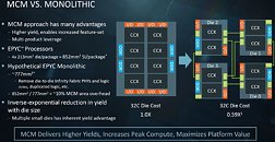
AMD, in its technical presentation for the new Radeon RX 7900 series "Navi 31" GPU, gave us an elaborate explanation on why it had to take the chiplets route for high-end GPUs, devices that are far more complex than CPUs. The company also enlightened us on what sets chiplet-based packages apart from classic multi-chip modules (MCMs). An MCM is a package that consists of multiple independent devices sharing a fiberglass substrate.

An example of an MCM would be a mobile Intel Core processor, in which the CPU die and the PCH die share a substrate. Here, the CPU and the PCH are independent pieces of silicon that can otherwise exist on their own packages (as they do on the desktop platform), but have been paired together on a single substrate to minimize PCB footprint, which is precious on a mobile platform. A chiplet-based device is one where a substrate is made up of multiple dies that cannot otherwise independently exist on their own packages without an impact on inter-die bandwidth or latency. They are essentially what should have been components on a monolithic die, but disintegrated into separate dies built on different semiconductor foundry nodes, with a purely cost-driven motive.

Eliyan Closes $40M Series A Funding Round and Unveils Industry's Highest Performance Chiplet Interconnect Technologies

Eliyan Corporation, credited for the invention of the semiconductor industry's highest-performance and most efficient chiplet interconnect, today announced two major milestones in the commercialization of its technology for multi-die chiplet integration: the close of its Series A $40M funding round, and the successful tapeout of its technology on an industry standard 5-nanometer (nm) process.

Eliyan's NuLink PHY and NuGear technologies address the critical need for a commercially viable approach to enabling high performance and cost-effectiveness in the connection of homogeneous and heterogenous architectures on a standard, organic chip substrate. It has proven to achieve similar bandwidth, power efficiency, and latency as die-to-die implementations using advanced packaging technologies, but without the other drawbacks of specialized approaches.

AMD Ready with Zen 4 3DV Cache Chiplet, Expects to Repeat 5800X3D Magic Versus Raptor Lake

AMD is allegedly ready with a working "Zen 4" chiplet that has stacked 3D Vertical Cache (3DV cache) memory, which supplements the on-die L3 cache, and is found to massively improve gaming performance. "Moore's Law is Dead" reports that the Zen 4 + 3DV Cache chiplet will be used with various Ryzen 7000X3D SKUs, as well as special EPYC "Genoa" SKUs.

The 3DV Cache deployed with the "Zen 4" chiplet is a second-generation to the one on the "Zen 3 + 3DV cache" chiplet, and AMD has worked on a number of bandwidth and latency improvements, so it performs in-sync with the generationally-faster on-die L3 cache of the "Zen 4" chiplet. Unlike the CCD below it that's built on TSMC N5 (5 nm EUV), the L3D (the stacked die with the 3DV cache) is possibly be built on an older node, such as N6 (6 nm), since it only contains a slab of memory and doesn't warrant N5. "Moore's Law is Dead" reports that AMD expects to repeat the magic of the 5800X3D when it comes to gaming performance, and expects Ryzen 7000X3D processors to dominate Intel's 13th Gen "Raptor Lake" processors. This was echoed by another reliable source, greymon55.

AMD RDNA3 Offers Over 50% Perf/Watt Uplift Akin to RDNA2 vs. RDNA; RDNA4 Announced

AMD in its 2022 Financial Analyst Day presentation claimed that it will repeat the over-50% generational performance/Watt uplift feat with the upcoming RDNA3 graphics architecture. This would be a repeat of the unexpected return to the high-end and enthusiast market-segments of AMD Radeon, thanks to the 50% performance/Watt uplift of the RDNA2 graphics architecture over RDNA. The company also broadly detailed the various new specifications of RDNA3 that make this possible.

To begin with, RDNA3 debuts on the TSMC N5 (5 nm) silicon fabrication node, and will debut a chiplet-based approach that's somewhat analogous to what AMD did with its 2nd Gen EPYC "Rome" and 3rd Gen Ryzen "Matisse" processors. Chiplets packed with the GPU's main number-crunching and 3D rendering machinery will make up chiplets, while the I/O components, such as memory controllers, display controllers, media engines, etc., will sit on a separate die. Scaling up the logic dies will result in a higher segment ASIC.

NVIDIA Opens NVLink for Custom Silicon Integration

Enabling a new generation of system-level integration in data centers, NVIDIA today announced NVIDIA NVLink -C2C, an ultra-fast chip-to-chip and die-to-die interconnect that will allow custom dies to coherently interconnect to the company's GPUs, CPUs, DPUs, NICs and SOCs. With advanced packaging, NVIDIA NVLink-C2C interconnect would deliver up to 25x more energy efficiency and be 90x more area-efficient than PCIe Gen 5 on NVIDIA chips and enable coherent interconnect bandwidth of 900 gigabytes per second or higher.

"Chiplets and heterogeneous computing are necessary to counter the slowing of Moore's law," said Ian Buck, vice president of Hyperscale Computing at NVIDIA. "We've used our world-class expertise in high-speed interconnects to build uniform, open technology that will help our GPUs, DPUs, NICs, CPUs and SoCs create a new class of integrated products built via chiplets."

Rumor: AMD Ryzen 7000 (Raphael) to Introduce Integrated GPU in Full Processor Lineup

The rumor mill keeps crushing away; in this case, regarding AMD's plans for their next-generation Zen designs. Various users have shared pieces of the same AMD roadmap, which apparently places AMD in an APU-focused landscape come their Ryzen 7000 series. we are currently on AMD's Ryzen 5000-series; Ryzen 6000 is supposed to materialize via a Zen 3+ design, with improved performance per watt obtained from improvements to its current Zen 3 family. However, Ryzen 7000-series is expected to debut on AMD's next-gen platform (let's call it AM5), which is also expected to introduce DDR5 support for AMD's mainstream computing platform. And now, the leaked, alleged roadmaps paint a Zen 4 + Navi 2 APU series in the works for AMD's Zen 4 debut with Raphael - roadmapped for manufacturing at the 5 nm process.

The inclusion of an iGPU chip with AMD's mainstream processors may signal a move by AMD to produce chiplets for all of its products, and then integrating them in the final product. You just have to think about it in the sense that AMD could "easily" pair one of the eight-core chiplets from the current Ryzen 5800X, for example, with an I/O die (which would likely still be fabricated with Global Foundries) an an additional Navi 2 GPU chiplet. It makes sense for AMD to start fabricating GPUs as chiplets as well - AMD's research on MCM (Multi-Chip Module) GPUs is pretty well-known at this point, and is a given for future development. It means that AMD needed only to develop one CPU chiplet and one GPU chiplet which they can then scale on-package by adding in more of the svelte pieces of silicon - something that Intel still doesn't do, and which results in the company's monolithic dies.

AMD Patents Chiplet-based GPU Design With Active Cache Bridge

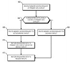
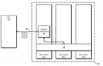
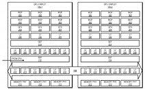
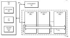
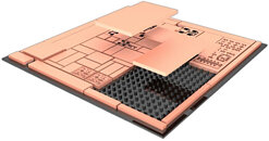
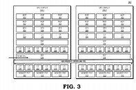
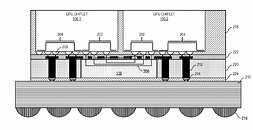
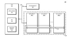
AMD on April 1st published a new patent application that seems to show the way its chiplet GPU design is moving towards. Before you say it, it's a patent application; there's no possibility for an April Fool's joke on this sort of move. The new patent develops on AMD's previous one, which only featured a passive bridge connecting the different GPU chiplets and their processing resources. If you want to read a slightly deeper dive of sorts on what chiplets are and why they are important for the future of graphics (and computing in general), look to this article here on TPU.

The new design interprets the active bridge connecting the chiplets as a last-level cache - think of it as L3, a unifying highway of data that is readily exposed to all the chiplets (in this patent, a three-chiplet design). It's essentially AMD's RDNA 2 Infinity Cache, though it's not only used as a cache here (and for good effect, if the Infinity Cache design on RDNA 2 and its performance uplift is anything to go by); it also serves as an active interconnect between the GPU chiplets that allow for the exchange and synchronization of information, whenever and however required. This also allows for the registry and cache to be exposed as a unified block for developers, abstracting them from having to program towards a system with a tri-way cache design. There are also of course yield benefits to be taken here, as there are with AMD's Zen chiplet designs, and the ability to scale up performance without any monolithic designs that are heavy in power requirements. The integrated, active cache bridge would also certainly help in reducing latency and maintaining chiplet processing coherency.
AMD Chiplet Design Patent with Active Cache Hierarchy AMD Chiplet Design Patent with Active Cache Hierarchy AMD Chiplet Design Patent with Active Cache Hierarchy AMD Chiplet Design Patent with Active Cache Hierarchy

AMD Files Patent for Chiplet Machine Learning Accelerator to be Paired With GPU, Cache Chiplets

AMD has filed a patent whereby they describe a MLA (Machine Learning Accelerator) chiplet design that can then be paired with a GPU unit (such as RDNA 3) and a cache unit (likely a GPU-excised version of AMD's Infinity Cache design debuted with RDNA 2) to create what AMD is calling an "APD" (Accelerated Processing Device). The design would thus enable AMD to create a chiplet-based machine learning accelerator whose sole function would be to accelerate machine learning - specifically, matrix multiplication. This would enable capabilities not unlike those available through NVIDIA's Tensor cores.

This could give AMD a modular way to add machine-learning capabilities to several of their designs through the inclusion of such a chiplet, and might be AMD's way of achieving hardware acceleration of a DLSS-like feature. This would avoid the shortcomings associated with implementing it in the GPU package itself - an increase in overall die area, with thus increased cost and reduced yields, while at the same time enabling AMD to deploy it in other products other than GPU packages. The patent describes the possibility of different manufacturing technologies being employed in the chiplet-based design - harkening back to the I/O modules in Ryzen CPUs, manufactured via a 12 nm process, and not the 7 nm one used for the core chiplets. The patent also describes acceleration of cache-requests from the GPU die to the cache chiplet, and on-the-fly usage of it as actual cache, or as directly-addressable memory.

AMD is Allegedly Preparing Navi 31 GPU with Dual 80 CU Chiplet Design

AMD is about to enter the world of chiplets with its upcoming GPUs, just like it has been doing so with the Zen generation of processors. Having launched a Radeon RX 6000 series lineup based on Navi 21 and Navi 22, the company is seemingly not stopping there. To remain competitive, it needs to be in the constant process of innovation and development, which is reportedly true once again. According to the current rumors, AMD is working on an RDNA 3 GPU design based on chiplets. The chiplet design is supposed to feature two 80 Compute Unit (CU) dies, just like the ones found inside the Radeon RX 6900 XT graphics card.

Having two 80 CU dies would bring the total core number to exactly 10240 cores (two times 5120 cores on Navi 21 die). Combined with the RDNA 3 architecture, which brings better perf-per-watt compared to the last generation uArch, Navi 31 GPU is going to be a compute monster. It isn't exactly clear whatever we are supposed to get this graphics card, however, it may be coming at the end of this year or the beginning of the following year 2022.

AMD Patents Chiplet Architecture for Radeon GPUs

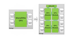
On December 31st, AMD's Radeon group has filed a patent for a chiplet architecture of the GPU, showing its vision about the future of Radeon GPUs. Currently, all of the GPUs available on the market utilize the monolithic approach, meaning that the graphics processing units are located on a single die. However, the current approach has its limitations. As the dies get bigger for high-performance GPU configurations, they are more expensive to manufacture and can not scale that well. Especially with modern semiconductor nodes, the costs of dies are rising. For example, it would be more economically viable to have two dies that are 100 mm² in size each than to have one at 200 mm². AMD realized that as well and has thus worked on a chiplet approach to the design.

AMD reports that the use of multiple GPU configuration is inefficient due to limited software support, so that is the reason why GPUs were kept monolithic for years. However, it seems like the company has found a way to go past the limitations and implement a sufficient solution. AMD believes that by using its new high bandwidth passive crosslinks, it can achieve ideal chiplet-to-chiplet communication, where each GPU in the chiplet array would be coupled to the first GPU in the array. All the communication would go through an active interposer which would contain many layers of wires that are high bandwidth passive crosslinks. The company envisions that the first GPU in the array would communicably be coupled to the CPU, meaning that it will have to use the CPU possibly as a communication bridge for the GPU arrays. Such a thing would have big latency hit so it is questionable what it means really.

CEA-Leti Makes a 96 core CPU from Six Chiplets

Chiplet design of processors is getting more popular due to many improvements and opportunities it offers. Some of the benefits include lower costs as the dies are smaller compared to one monolithic design, while you are theoretically able to stitch as much of the chiplets together as possible. During the ISSCC 2020 conference, CEA-Leti, a French research institute, created a 96 core CPU made from six 3D stacked 16 core chiplets. The chip is created as a demonstration of what this modular approach offers and what are the capabilities of the chiplet-based CPU design.

The chiplets are manufactured on the 28 nm FD-SOI manufacturing process from STMicroelectronics, while the active interposer die below them that is connecting everything is made using the 65 nm process. Each one of the six dies is housing 16 cores based on MIPS Instruction Set Architecture core. Each chiplet is split into four 4-core clusters that make up for a total of 16 cores per chiplet. When it comes to the core itself, it is a scalar MIPS32v1 core equipped with 16 KiB of L1 instruction and an L1 data cache. For L2 cache, there is 256 KiB per cluster, while the L3 cache is split into four 1 MiB tiles for the whole cluster. The chiplets are stacked on top of an active interposer which connects the chiplets and provides external I/O support.

AMD Gives Itself Massive Cost-cutting Headroom with the Chiplet Design

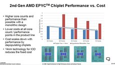
At its 2020 IEEE ISSCC keynote, AMD presented two slides that detail the extent of cost savings yielded by its bold decision to embrace the MCM (multi-chip module) approach to not just its enterprise and HEDT processors, but also its mainstream desktop ones. By confining only those components that tangibly benefit from cutting-edge silicon fabrication processes, namely the CPU cores, while letting other components sit on relatively inexpensive 12 nm, AMD is able to maximize its 7 nm foundry allocation, by making it produce small 8-core CCDs (CPU complex dies), which add up to AMD's target core-counts. With this approach, AMD is able to cram up to 16 cores onto its AM4 desktop socket using two chiplets, and up to 64 cores using eight chiplets on its SP3r3 and sTRX4 sockets.

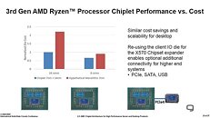
In the slides below, AMD compares the cost of its current 7 nm + 12 nm MCM approach to a hypothetical monolithic die it would have had to build on 7 nm (including the I/O components). The slides suggest that the cost of a single-chiplet "Matisse" MCM (eg: Ryzen 7 3700X) is about 40% less than that of the double-chiplet "Matisse" (eg: Ryzen 9 3950X). Had AMD opted to build a monolithic 7 nm die that had 8 cores and all the I/O components of the I/O die, such a die would cost roughly 50% more than the current 1x CCD + IOD solution. On the other hand, a monolithic 7 nm die with 16 cores and I/O components would cost 125% more. AMD hence enjoys a massive headroom for cost-cutting. Prices of the flagship 3950X can be close to halved (from its current $749 MSRP), and AMD can turn up the heat on Intel's upcoming Core i9-10900K by significantly lowering price of its 12-core 3900X from its current $499 MSRP. The company will also enjoy more price-cutting headroom for its 6-core Ryzen 5 SKUs than it did with previous-generation Ryzen 5 parts based on monolithic dies.

AMD Doubles L3 Cache Per CCX with Zen 2 "Rome"

A SiSoft SANDRA results database entry for a 2P AMD "Rome" EPYC machine sheds light on the lower cache hierarchy. Each 64-core EPYC "Rome" processor is made up of eight 7 nm 8-core "Zen 2" CPU chiplets, which converge at a 14 nm I/O controller die, which handles memory and PCIe connectivity of the processor. The result mentions cache hierarchy, with 512 KB dedicated L2 cache per core, and "16 x 16 MB L3." Like CPU-Z, SANDRA has the ability to see L3 cache by arrangement. For the Ryzen 7 2700X, it reads the L3 cache as "2 x 8 MB L3," corresponding to the per-CCX L3 cache amount of 8 MB.

For each 64-core "Rome" processor, there are a total of 8 chiplets. With SANDRA detecting "16 x 16 MB L3" for 64-core "Rome," it becomes highly likely that each of the 8-core chiplets features two 16 MB L3 cache slices, and that its 8 cores are split into two quad-core CCX units with 16 MB L3 cache, each. This doubling in L3 cache per CCX could help the processors cushion data transfers between the chiplet and the I/O die better. This becomes particularly important since the I/O die controls memory with its monolithic 8-channel DDR4 memory controller.

On The Coming Chiplet Revolution and AMD's MCM Promise

With Moore's Law being pronounced as within its death throes, historic monolithic die designs are becoming increasingly expensive to manufacture. It's no secret that both AMD and NVIDIA have been exploring an MCM (Multi-Chip-Module) approach towards diverting from monolithic die designs over to a much more manageable, "chiplet" design. Essentially, AMD has achieved this in different ways with its Zen line of CPUs (two CPU modules of four cores each linked via the company's Infinity Fabric interconnect), and their own R9 and Vega graphics cards, which take another approach in packaging memory and the graphics processing die in the same silicon base - an interposer.
Return to Keyword Browsing
Nov 21st, 2024 11:16 EST change timezone

New Forum Posts

Popular Reviews

Controversial News Posts