News Posts matching #Clarkdale

Return to Keyword Browsing

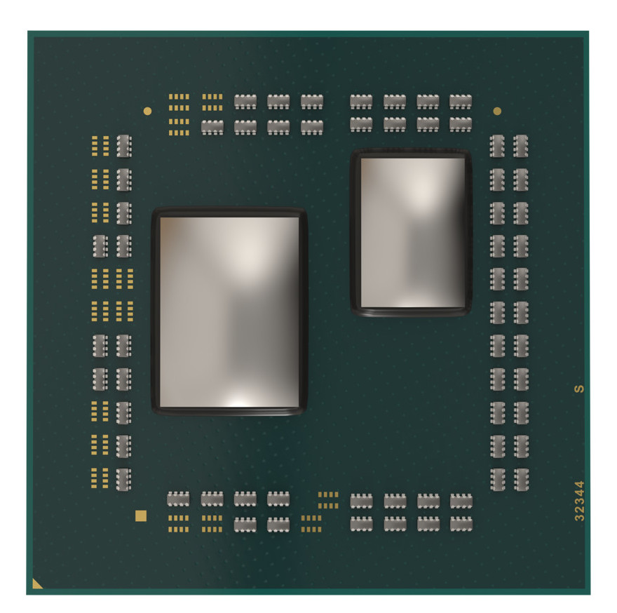
AMD Confirms Ryzen 3000 "Matisse" Features Soldered IHS

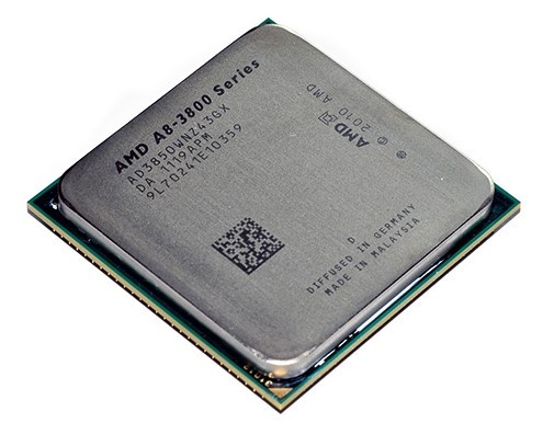
AMD senior technical marketing manager Robert Hallock, responding to a specific question on Twitter, confirmed that the 3rd generation Ryzen processors do feature soldered integrated heatspreaders (IHS). Soldering as an interface material is preferred as it offers better heat transfer between the processor die and the IHS, as opposed to using a fluid TIM such as pastes. "Matisse" will be one of the rare few examples of a multi-chip module with a soldered IHS. The package has two kinds of dies, one or two 7 nm "Zen 2" 8-core CPU chiplets, and one 14 nm I/O Controller die.

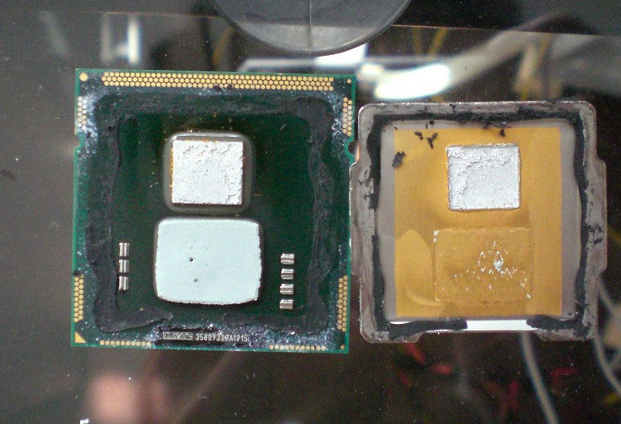
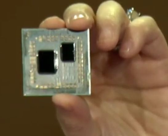
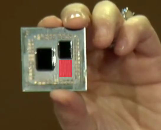
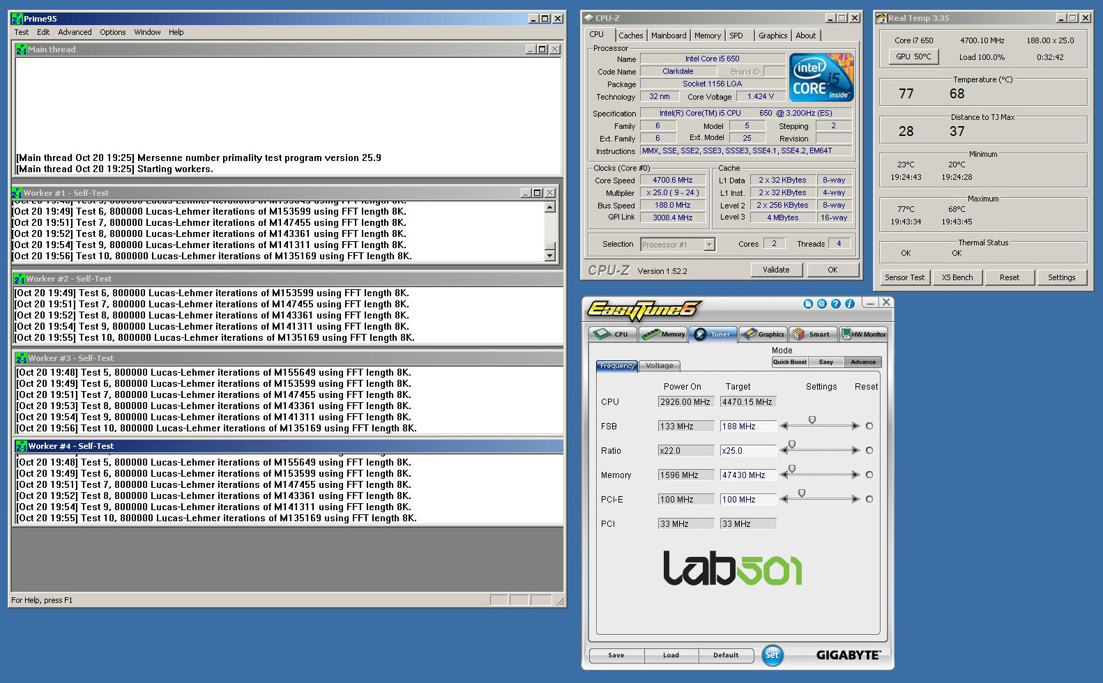
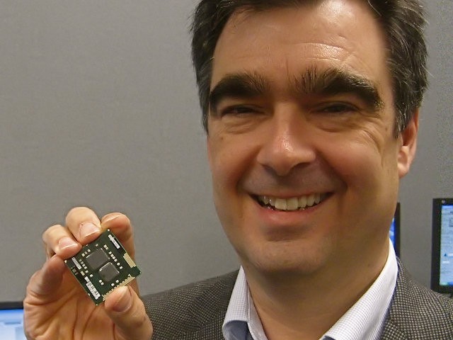
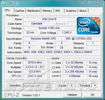
The most similar example of such a processor would be Intel's "Clarkdale" (pictured below), which has its CPU cores sitting on a 32 nm die, while the I/O, including memory controller and iGPU, are on a separate 45 nm die. On-package QPI connects the two. Interestingly, Intel used two different sub-IHS interface materials for "Clarkdale." While the CPU die was soldered, a fluid TIM was used for the I/O controller die. It would hence be very interesting to see if AMD solders both kinds of dies under the "Matisse" IHS, or just the CPU chiplets. Going by Hallock's strong affirmative "Like a boss," we lean toward the possibility of all dies being soldered.
Image Credit: TheLAWNOOB (OCN Forums)

AMD 3rd Gen Ryzen AM4 Package Capable of Two 8-core Chiplets

At its CES 2019 keynote, AMD unveiled two killer client-segment products, the Radeon VII graphics card, which beats the GeForce RTX 2080; and a sneak preview of the 3rd generation Ryzen socket AM4 processor based on the company's "Zen 2" microarchitecture. As part of the unveil, CEO Lisa Su demonstrated an 8-core/16-thread 3rd generation Ryzen prototype processor in a head-to-head CineBench nT face-off with the Intel Core i9-9900K processor, which has the same core-count. The Ryzen narrowly beat the Intel flagship. Following this, Dr. Su held up a de-lidded sibling of the processor that was tested, revealing not one, but two dies.

This confirms that AMD is taking the heterogeneous multi-chip module approach to building its 3rd generation Ryzen processors, much like its 2nd generation EPYC processors that were unveiled late last year. The MCM of the processor Dr. Su held up had two chips, the smaller chip is an 8-core CPU chiplet built on the 7 nm process, that appears to have the same die-size as the 8-core chiplets that make up the 64-core 2nd gen EPYC MCMs, the larger die is an I/O controller logic built on the 14 nm process. This die controls the memory, PCIe, and SoC connectivity of the package. We noticed something curious about the way the two dies are arranged on the package substrate.

Intel Core "Coffee Lake" Lineup Specs Confirmed in Leaked Distributor Event

Intel recently concluded an event intended for local distributors in China, a key presentation slide of which was snapped and posted online. The slide confirms the company's product-stack for the mainstream desktop platform, and its augmentation with the first wave of 8th generation Core "Coffee Lake" SKUs. The slide also confirms that Intel will be replacing current Core i7 4-core/8-thread SKUs with Core i7 6-core/12-thread ones; Core i5 4-core/4-thread SKUs with 6-core/6-thread ones, and Core i3 2-core/4-thread SKUs with 4-core/4-thread ones, marking the biggest fundamental update to the product stack since the Core MSDT family started out a decade ago, with the Core "Lynnfield" and "Clarkdale" processors.

The slide further describes per-core performance increases ranging between 11-29 percent owing to higher clock-speeds and a slightly newer micro-architecture, and 51-65 percent increases in multi-threaded performance owing to the increasing core-counts across the board. While these SKUs are expected to logically replace the various Core "Kaby Lake" SKUs from their current price-points, there could be a tiny price increase, across the board, which Intel could justify using the higher core-counts.

AMD Faces Securities Fraud Lawsuit

Over-promising and under-delivering with its very first accelerated processing units (APU), codenamed "Llano," is coming back to haunt AMD, with a US District Court ruling that the company must face claims from investors over potential securities fraud. Launched in Q3-2012, AMD's A-series "Llano" APUs went largely unsold due to various factors including lack of product appeal, competition from Intel, forcing AMD to pull in its second-generation "Trinity" APU too soon. The related development first took shape in January 2014.

The swelling unsold "Llano" inventory forced an inventory writedown of $100 million, reducing the company's worth by nearly that much overnight, and tanking the value of the AMD stock. While AMD talked about the concept of an APU for years, Intel was the first to come out with a processor that integrates a graphics processor, with its Core i3 and Core i5 "Clarkdale" processors. The suit claims that AMD misrepresented production of "Llano" chips to its investors despite supply issues from its foundry partner GlobalFoundries, artificially inflating the value of the company in 2011-12. By the time production finally caught up, it ended up overproducing resulting in unsold inventory, and in consequence, the $100 million writeoff.

Some Intel LGA1156, LGA775 Processors to be Discontinued

Intel is preparing to discontinue a couple of Core processors in the LGA1156 package, and a few older processors in the LGA775 package. These include the Core i5-661 and Core i3-530, two of the first Clarkdale dual-core processors, Pentium Dual-Core E5700, Celeron E3500 and E3400.

Intel will take orders for Core i5-661 and Core i3-530 till April 27, 2012, and will ship the last of them by October 5, 2012. Orders for Pentium E5700, Celeron E3500 and Celeron E3400 will be taken till December 30, 2011. While the last of the tray shipments will be completed by June 8th, 2012, boxed versions will ship till supplies are depleted in Intel's warehouses.

Intel Gives Core i3 and Core i5 Dual-Core Processors K0 Stepping Update

Intel is giving some existing 32 nm "Clarkdale" based Core i3 and Core i5 processors an update. The processors will transition to the new K0 stepping from the existing C2 stepping. The parts that will be made on the K0 silicon are Core i3 models 530 (new sSPEC: SLBX7), 540 (new sSPEC: SLBTD) and Core i5 models 650 (new sSPEC: SLBTJ), 660/661 (SLBTK/SLBTB), 670 (SLBTL). Newer and upcoming models such as the i3-550, i3-560, i5-665K, and i5-680 are already being built on the K0 stepping die. Motherboards will require a BIOS update to support the new K0 stepping processors.

The K0 stepping change includes the following highlights:
  • New S-spec and MM numbers for the converting products
  • Extended CPUID will change from 0x00020652 to 0x00020655
  • Host RevID will change from 0x12 to 0x18
  • K0 stepping package is pin compatible with C2 stepping package
  • Adds Processor Context ID (PCID) support
The revised older SKUs that are built on K0 stepping will be market-available by October 16.

Intel Wants $50 for Software Unlock of CPU Features

The Pentium G6951 dual-core LGA1156 processor may not have made any headlines when it was known to be almost identical to the Pentium G6950, until now. Intel designed the G6951 to support "hardware feature upgrades" by purchasing them and enabling them using a software, so users with this processor installed can upgrade their systems by enabling that are otherwise locked for the SKU. The $50 upgrade fetches support for HyperThreading Technology, enabling four threads on the processor; and unlocks the disabled 1 MB of the L3 cache (Clarkdale has 4 MB of L3 cache, of which 1 MB is disabled on the Pentium SKUs).

There isn't much value in buying a $99 Pentium G6951 and the $50 Upgrade Card upfront, but later down the line, companies can opt to mass-upgrade system performance without touching any of the hardware inside. The service works by the purchase of an upgrade key that the user has to feed into the software, which is then verified by Intel's activation server, following successful verification, the software unlocks the processor's features. This is a one-time process, portable between software reinstallations.

Intel Releases Core i7 875K and Core i5 655K, Lures Overclockers with Pricing

Intel today rolled out two new high-performance processors aimed at the enthusiast community, which is sure to please users of LGA1156 platform. The release includes the quad-core Core i7 875K, and dual-core Core i5 655K. Based on the 45 nm Lynnfield die, the Core i7 875K is clocked at 2.93 GHz, with a maximum Turbo Boost speed of 3.60 GHz. While having identical clock speeds to the Core i7 870, the 875K comes with a fully unlocked BClk multiplier, which is featured in Extreme Edition processors.

The unlocked multiplier helps with overclocking. Also featured is that the core and DRAM ratios are unlocked so memory bus speeds can be kept independent of the core speed to an extant. The processor retains the TDP rating of 95W, which other Lynnfield-based processors have. It has a monolithic die which houses the processor and northbridge, dual-channel DDR3 memory controller, and PCI-Express root complex. Intel HyperThreading Technology enables 8 logical CPUs for the OS to deal with.

Intel Intros Core i5 680 and Pentium E5500

Intel introduced two new dual-core processors, the high-end Core i5 680, and the value-segment Pentium Dual-Core E5500. The former is an LGA1156 chip that runs on Intel P55, H55, H57, Q55, Q57 chipsets, while the latter is an LGA775 chip that works on most recent LGA775 motherboards. The Core i5 680 uses the 32 nm based Clarkdale core. At 3.60 GHz (27 x 133 MHz) with a Turbo Boost speed of 3.86 GHz, the i5 680 is expected to be the fastest dual-core processor ever made. Its embedded Intel HD Graphics controller is clocked at 733 MHz. It has L2 caches of 256 KB per core, and a shared L3 cache of 4 MB. It supports two channels of DDR3 memory. With HyperThreading enabled, the chip gives the OS four logical CPUs to deal with. It has a TDP of 73W.

The Pentium Dual-Core E5500 is based on the 45 nm Wolfdale-2M core, it has a clock speed of 2.80 GHz (14 x 200 MHz), and FSB speed of 800 MHz. It has a shared L2 cache of 2 MB, and TDP of 65W. While the Core i5 680 is priced at US $294, the E5500 goes for $75. All prices are per-piece in 1000 unit tray quantities.

Intel Readying Core i7 875K and Core i5 655K Overclocker-Friendly LGA1156 Processors

Intel carved out high-end socket LGA1156 processors such as the Core i7 800 series, just so people opting for the LGA1156 also have the headroom to upgrade to high-end parts without having to switch to the more powerful LGA1366 platform with its Core i7 900 series processors. There are four parts in the performance-enthusiast (>$250) segment: Core i5 670 dual-core, Core i7 860 and Core i7 870 quad-core. With the possible advent of more powerful socket AM3 processors from AMD, notably the Phenom II X6 series with its overclocker-friendly Black Edition parts, Intel seems to be finding a need to expand its LGA1156 series a little.

In the works are the Core i7 875K quad-core, and Core i5 655K dual-core. Being careful as to not label them "Extreme Edition" chips (since the "Extreme Edition" moniker seems to be clearly demarcated for the LGA1366 platform and the market segment by that name), Intel gave these chips the "K" brand identifier. Last summer, Intel released the Pentium Dual-Core E6500K to select markets. Similar to that, the Core i7 875K and Core i5 655K are overclocker-friendly chips that come with unlocked BClk multipliers (much like the Extreme Edition chips).

ASUS Introduces P7F7-E SuperComputer Motherboard with Next-Gen Connectivity Features

ASUS today announced the launch of the new ASUS P7F7-E WS SuperComputer motherboard which maximizes transmission speeds by integrating the industry's latest I/O technologies such as USB 3.0, SATA 6G storage interface, and IEEE 1394b FireWire standard. Additionally, the ASUS P7F7-E WS SuperComputer is equipped with the LGA1156 socket and the latest Intel 3450 chipset with onboard graphics. For extreme gaming enjoyment, up to four ATI CrossFireX cards or 3-way/2-way NVIDIA SLI cards can be accommodated to generate smoother and sharper visuals. It also leverages NVIDIA CUDA parallel computing architecture to support up to four NVIDIA Tesla cards with Clarkdale Processors for intensive high-performance computing.

The ASUS P7F7-E WS SuperComputer is the best choice for providing comprehensive I/O support. It includes USB 3.0 ports-the latest connectivity standard with 4.8Gb/s speeds-to support next-generation components and peripherals. USB 3.0 transfers data ten times faster and is backward compatible with USB 2.0 components. Additionally, the ASUS P7F7-E WS SuperComputer includes Serial ATA (SATA) 6Gb/s storage interfaces for 6.0Gbps data throughput, thus enhancing scalability, accelerating data retrieval, and doubling the bandwidth of current bus systems. To support FireWire-enabled digital video recorders and computers, the ASUS P7F7-E WS SuperComputer also includes two IEEE 1394b ports supporting up to 800 Mb/s speeds-doubling the previous IEEE 1394a speeds.

TechPowerUp GPU-Z 0.3.9 Released

TechPowerUp today released GPU-Z version 0.3.9, our graphics subsystem information and monitoring utility. The new version brings with it some important user-interface changes that make it accessible to various locales and language settings. It adds support for over 32 new graphics processors by AMD and NVIDIA, and a host of new technical improvements that make it more stable and accurate.

DOWNLOAD: TechPowerUp GPU-Z 0.3.9

A list of changes are as follows:

Upcoming Intel Core CPUs Detailed

Intel is poised to release new performance and high-end processors across its various Core family brands, within Q1 2010 and later. OCWorkbench, citing sources in Japan, released tentative release dates and information of new Core family processors. Among a few known names such as the six-core Core i7 980X, there are a few new ones. Details and dates are as follows:
  • Core i7 980X "Gulftown": six-core, LGA-1366, 3.33 GHz (turbo: 3.60 GHz), March 16
  • Core i7 970 "Bloomfield": quad-core, LGA-1366, 3.33 GHz (turbo: 3.46 GHz), Q3, 2010
  • Core i7 930 "Bloomfield": quad-core, LGA-1366, 2.80 GHz (turbo: 3.06 GHz), February 28
  • Core i7 880 "Lynnfield": quad-core, LGA-1156, 3.06 GHz (turbo: 3.73 GHz), Q2, 2010
  • Core i5 680 "Clarkdale": dual-core, LGA-1156, 3.60 GHz (turbo: 3.80 GHz), Mid-May
  • Core i3 550 "Clarkdale": dual-core, LGA-1156, 3.20 GHz, Q2, 2010
  • Pentium E6700 "Wolfdale-2M": dual-core, LGA-775, 3.43 GHz, Q2, 2010
Although the Core i7 960 is available in its OEM form, the company doesn't plan to retail it with its retail packaging.

BIOSTAR Introduces the TH55B HD Motherboard

Followed by Intel recent 32nm "Clarkdale" Core i5 / i3 processor launch with built-in GPU engine, it is now a brand new page and competition for all-in-one PC. BIOSTAR, a professional manufacturer of motherboards after its top-line H55 motherboards "TH55XE" being released, today we see another main stream board "TH55B HD" in the market remains high quality component design, outstanding over clocking capabilities and new colorful slots. And of course, it also offers more competitive prices.

"TH55B HD" - a member of BIOSTAR famous "T-Series" with Micro ATX form factor design, black color PCB, and supporting latest Intel 32nm "Clarkdale" Core i5 / i3 processor.

GIGABYTE Launches H55/H57 Series Motherboards with USB 3.0 and DisplayPort Interface

GIGABYTE TECHNOLOGY Co., Ltd, a leading manufacturer of motherboards, graphics cards and other computing hardware solutions is pleased to announce their latest generation H55/H57 series motherboards, based on the Intel H55 and Intel H57 chipset and leveraging the success of the GIGABYTE Ultra Durable 3 design featuring 2x copper PCB and delivering a host of cutting-edge features including innovative Smart6 PC management tools, Dynamic Energy Saver 2 power saving utilities, DualBIOS and support for Energy Using Products Directive (EuP), for a powerful, yet power efficient multimedia platform.

"GIGABYTE once again leads the motherboard industry and sets the standard for delivering high speed data transfer and richer video playback capabilities for HD multimedia home entertainment devices," commented Tim Handley, Deputy Director of Motherboard Marketing at GIGABYTE Technology Co. Ltd. "Featuring next generation storage capabilities including USB 3.0 and high performance digital DisplayPort connectivity, as well as GIGABYTE's own unique 3x USB Power Boost, the GIGABYTE GA-H57M-USB3 and GA-H55M-USB3 provide a compelling solution for users wanting the ultimate multimedia system."

Intel Unveils Core i5 6xx, 6x1 Series Dual-Core Processors

Intel today gave a go ahead for the media to publish reviews of its brand new dual-core processors under the Core i5 6xx and Core i5 6x1 series. The processors are based on the new "Clarkdale" processor die, and make use of the company's 32 nm next generation HKMG manufacturing process. Unlike conventional processor packages based on the Nehalem/Westmere architecture, the new processors move the northbridge component of the system onto the processor package, only that it is based on a separate 45 nm die within the package. The 32 nm processor die houses two processor cores along with up to 4 MB of L3 cache, while it is wired to a larger iGPU die which houses the dual-channel DDR3 memory controller, a graphics core, PCI-Express root complex, along with other components traditionally found on northbridge chips.

The first three models in the new Core i5 series are the 3.20 GHz Core i5 650, 3.33 GHz Core i5 660 and 661 (latter has a faster iGPU), and 3.46 GHz Core i5 670. These processors have the LGA-1156 package and are compatible with existing P55 Express chipset (albeit without the iGPU feature), along with the company's new H55 Express and H57 Express chipsets that support the Flexible Display Interface that provides connectivity to the processors' iGPUs. The new processors feature HyperThreading Technology, with which it provides the operating system with four logical CPUs (threads) to deal with, TurboBoost technology which powers down a core and overclocks the other when the task load is low. Pricing and availability will surface when the processors are formally announced, a little later this month. Meanwhile, motherboard manufacturers are ready with boatloads of new motherboard models based on Intel's two new chipsets. A compilation of links to major reviews on the internet can be found in the day's reviews list on the homepage.

Core i5 650 ''Clarkdale'' Reaches 4.70 GHz on Air-Cooling

Intel's socket LGA-1156 quad-core processors are closely trailed by the company's first processors based on the 32 nm manufacturing process: Core i5 and Core i3 "Clarkdale" dual-core processors. Engineering samples of these processors were evaluated as early as Q2 2009, but one of the first attempts to show the processors' overclocking potential using air-cooling was made very recently. Even prior to that, a low-voltage overclocking feat by Coolaler showed how engineering samples didn't particularly struggle reaching clock speeds close to 4.00 GHz with vCore as low as 0.832V. Romanian tech community Lab501. Lab501 community leader "Monstru" tested the overclocking headroom of a Core i5 650 LGA-1156 dual-core processor (engineering sample) with air-cooling.

The test-bed included a Gigabyte P55 motherboard, the Core i5 650 processor was cooled by a Noctua NH-U12P, onto which a Coolink SWIF 2 120P fan was strapped. A clock speed of 4.70 GHz (25 x 188 MHz) was achieved (nearly 50% over the stock clock speed of 3.20 GHz). A core voltage of 1.424V was used. A point here to note however, is that the retail Core i5 650 will come with an upwards-locked bus frequency multiplier of 24 (24 x 133 MHz = 3.20 GHz). The processor at 4.70 GHz, was Prime95-stable for over 30 minutes. With an ambient temperature of 24 °C, the two cores heated up to 77 and 68 °C, not to forget that the processor was being air-cooled. Although with the use of an engineering sample (since the retail launch of this processor is tentatively three months away), the scope for inference of this feat is limited, it gives you a coarse indication that Intel is keeping the trend of ferociously fast dual-core processors alive. High(er) overclocking headroom on air-cooling is the fruition of the 32 nm process. Slated for Q1 2010, the siblings (and cousins) of the Core i5 650 include Core i5 660/661 (3.33 GHz, HTT), Core i5 670 (3.46 GHz, HTT), Core i3 540 (3.06 GHz, no HTT), Core i3 530 (2.93 GHz, no HTT), and Pentium G6950 (2.80 GHz, no HTT). Details of the series can be found here.

Intel Commences 32 nm Chip Production

Intel's foundries have commenced mass production of the company's first processors based on the 32 nm second generation high-K metal gate (HKMG) technologies. With these the company's next-generation Westmere architecture becomes retail-grade. The first products will include dual-core processors compatible with the recently introduced socket LGA-1156 platforms, and will carry the brand identifiers (and model number schemes) Core i5 600 series, Core i3 500 series, and Pentium dual-core series.

The desktop-grade parts are based on the "Clarkdale" core, and notebook-grade ones "Arrandale". The latter will be introduced first among the two, with the first Arrandale chips slated for Q4 2009, while the desktop chips arrive a little later in Q1 2010. Intel will focus on this transition to the Westmere architecture in the upcoming Intel Developer Forum event.

Clarkdale IGP Detailed, Tested

Intel's upcoming "Clarkdale" is special for two reasons: it is the first 32 nm based processor from Intel, and that it's the first processor that comes with a graphics processor built in, something AMD conceptualized a long time ago. Under the hood (read: integrated heat-spreader), Clarkdale is a busy package, that holds a CPU complex die (that houses the main processing cores, cache, a dual-channel DDR3 integrated memory controller, and a Quickpath interconnect controller, that connects the die to its neighbor, a northbridge-iGraphics die that houses most northbridge components including a PCI-Express 2.0 root complex, the star-attraction IGP and a DMI connection to the "platform controller hub (PCH)".

Core i3, Core i5 Dual-Core Processor Model Numbers Surface

Intel is weeks away from letting loose its first socket LGA-1156 processors, starting with a series of quad-core models, namely Core i5 750, Core i7 860, and Core i7 870. According to the latest roadmaps, dual-core derivatives of the Westmere architecture, will arrive in early 2010. IT168 sourced details of the model numbers Intel chalked out, based on roadmap excepts. An older report detailed all six models based on the "Clarkdale" core, including three in the Core i5 series, two in the Core i3 series, and one in the Pentium Dual-Core series. Let's try to make sense of this branding structure.

Clarkdale 3.06 GHz Faces a Preview, Series Pricing Surfaces

"Clarkdale" is the codename for Intel's upcoming dual-core processors derived from the Nehalem/Westmere architecture. The move marks a leap for Intel in two ways: introducting the first commercial-grade 32 nm microprocessor, and implementing a radical new design that involved relocating the platform's northbridge component entirely to the CPU package. Slated for Q1 2010, Clarkdale will go by three brand indentifiers to grade it according to a performance and feature scale. You have the Core i5 class that enables the entire feature-set of processor, there's the Core i3 class that offers some features, excluding Intel Turbo Boost technology for example, finally there's the sub-$100 Pentium part (yes, Pentium lives on), which offers a smaller feature-set. HyperThreading technology is disabled on this one.

Chinese tech-site IT168 published a comprehensive performance (p)review of the 3.06 GHz Clarkdale part. In the article, the 3.06 GHz Clarkdale was pitted against the 3.00 GHz "Wolfdale" Core 2 Duo processor. The memory (Dual-channel DDR3-1333, 4 GB) and graphics hardware (ATI Radeon HD 4870, 1 GB) were kept common between the two test-beds. Tests ranged from memory and CPU internal bandwidth tests, math-intensive tests, synthetic multimedia and 3D tests, and finally, modern 3D games.

First Intel Clarkdale Core i3 Low-Voltage Overclocking Feat Yields 4 GHz at 0.832 V

Intel's upcoming dual-core derivatives of the Nehalem/Westmere architecture, codenamed "Clarkdale" seems to have some interesting electrical characteristics. The CPU component of the chip is built on Intel's brand new 32 nanometre process that facilitates higher transistor densities, and in the process, intends to bring down TDP. An overclocking feat by Coolaler.com seems to suggest one of two things: either these chips have naturally low vCore voltages, or that the overlocking headroom at low-voltages is exceptional. Coolaler used a pre-release engineering sample of the Core i3 Clarkdale processor on a compatible platform, and achieved 4 GHz of clock speed with the vCore at 0.832 V. The frequency multiplier of the CPU was set at 25.0x, and a bus speed of 160 MHz used. Intel will be ready with these processors by the end of this year.

Intel 32 nm Clarkdale Chip Brought Forward to Q4 2009

While the bulk of Intel's upcoming Nehalem and Westmere derived products include quad-core processors, the company hasn't left out dual-core processors just as yet. The dual-core Core i5 desktop processor will be based on the new Clarkdale core, built on the 32 nm Westmere architecture. Originally slated for a Q1 2010 launch, the new chip seems to have been pulled into the Q4 2009 launch schedule, deep enough to make for a significant amount of projected sales, according to sources in the Taiwanese motherboard industry.

The sales projections for Q4 look particularly interesting. Core i5 "Clarkdale" dual-core is projected to amount for 10% of Intel's sales, while Core i7 "Bloomfield" at 1%, Core i5 "Lynnfield" at 2% (Core i7 "Lynnfield" is slated for Q1 2010), Core 2 Quad at 9%, Core 2 Duo E7000/E8000 at 35%, Pentium E5000/E6000 at 31%, Celeron E3000 and Atom together at 9%, Pentium E2000 and Celeron 400 together at 4%. In the following quarter, Clarkdale's sales share is expected to rise to 20%. The numbers prove just how large the market for dual-core processors is, even four years into the introduction of quad-core chips.

Details on Intel's Core Brand Product Placement Emerge, Gulftown to be Named Core i9

Last week, Intel sketched out its strategy in dealing with its client processor brand Core, and placing its different kinds of processors in series of markers (such as "i3", "i5", and "i7"), on the merit of performance and features they offer, and not necessarily a segregation based on core type and socket type. This raised a big debate in our forums, on who is really going to benefit from this kind of branding.

Chinese website INPAI.com.cn sourced information which explains what factors go into determining which brand marker a processor gets. The table elaborates on how different kinds of Intel processors (determined by core and socket types) cross different lines, with a few features toggled or enhanced. It is sure to throw up some surprises.

Photos Emerge of Intel's 32 nm Clarkdale Processor

Not long after Intel was said to have sent out samples of its new 32 nm mainstream processor based on Nehalem micro-architecture, someone over at XS forums, has posted photos of an as yet unnamed Clarkdale processor, running at 2.4 GHz, with 4 MB L3 Cache. The only official information from Intel we have about these processors is what we covered two months ago, when Intel spread open its plans to deal with the mainstream and value markets using its Nehalem micro-architecture.
Return to Keyword Browsing
May 2nd, 2024 00:09 EDT change timezone

New Forum Posts

Popular Reviews

Controversial News Posts