News Posts matching #DARPA

Return to Keyword Browsing

Intel Joins DARPA's Space-BACN to Accelerate Inter-Satellite Communications

he U.S. Defense Advanced Research Projects Agency (DARPA) has selected Intel for Phase 1 of the Space-Based Adaptive Communications Node (Space-BACN) program, which aims to create a low-cost, reconfigurable optical communications terminal that will translate information between diverse satellite constellations. A Space-BACN satellite terminal will enable communications between satellite constellations, enabling data to be sent anywhere around the planet at the speed of light.

DARPA is planning for a future where tens of thousands of satellites from multiple private sector organizations deliver broadband services from low earth orbit (LEO). The goal of Space-BACN is to create an "internet" of satellites, enabling seamless communication between military/government and commercial/civil satellite constellations. The program will facilitate collaboration among partners to ensure that the terminal being designed is reconfigurable to provide interoperability among the participating constellation providers.

Intel and DARPA Develop Secure Structured ASIC Chips Made in the US

Intel and the U.S. Defense Advanced Research Projects Agency (DARPA) today announced a three-year partnership to advance the development of domestically manufactured structured Application Specific Integrated Circuit (ASIC) platforms. The Structured Array Hardware for Automatically Realized Applications (SAHARA) partnership enables the design of custom chips that include state-of-the-art security countermeasure technologies. A reliable, secure, domestic source of leading-edge semiconductors remains critical to the U.S.

"We are combining our most advanced Intel eASIC structured ASIC technology with state-of-the-art data interface chiplets and enhanced security protection, and it's all being made within the U.S. from beginning to end. This will enable defense and commercial electronics systems developers to rapidly develop and deploy custom chips based on Intel's advanced 10 nm semiconductor process," said José Roberto Alvarez, senior director, CTO Office, Intel Programmable Solutions Group.

Intel to Collaborate with Microsoft on DARPA Program

Intel today announced that it has signed an agreement with Defense Advanced Research Projects Agency (DARPA) to perform in its Data Protection in Virtual Environments (DPRIVE) program. The program aims to develop an accelerator for fully homomorphic encryption (FHE). Microsoft is the key cloud ecosystem and homomorphic encryption partner leading the commercial adoption of the technology once developed by testing it in its cloud offerings, including Microsoft Azure and the Microsoft JEDI cloud, with the U.S. government. The multiyear program represents a cross-team effort across multiple Intel groups, including Intel Labs, the Design Engineering Group and the Data Platforms Group, to tackle "the final frontier" in data privacy, which is computing on fully encrypted data without access to decryption keys.

"Fully homomorphic encryption remains the holy grail in the quest to keep data secure while in use. Despite strong advances in trusted execution environments and other confidential computing technologies to protect data while at rest and in transit, data is unencrypted during computation, opening the possibility of potential attacks at this stage. This frequently inhibits our ability to fully share and extract the maximum value out of data. We are pleased to be chosen as a technology partner by DARPA and look forward to working with them as well as Microsoft to advance this next chapter in confidential computing and unlock the promise of fully homomorphic encryption for all," said Rosario Cammarota, principal engineer, Intel Labs, and principal investigator, DARPA DPRIVE program.

Arm Spins-out Cerfe Labs to Advance Development of CeRAM Memory Technology

Today Arm announced the spin-out of Cerfe Labs to develop and license new types of non-volatile memories based on correlated electron materials (CeRAM) and ferroelectric transistors (FeFETs). Arm CeRAM researchers will join Cerfe Labs and assume ownership of the Arm joint development project with Symetrix Corporation.

As part of the spin-out, Arm will transfer its full CeRAM IP portfolio of more than 150 patent families to Cerfe Labs that will be the foundation for a roadmap of related CeRAM technologies. Cerfe Labs initial focus will be on producing meaningful prototypes which will be licensed to partners with a goal of accelerating timing of enabling these novel non-volatile materials for systems.

Arm and DARPA Sign Partnership Agreement to Accelerate Technological Innovation

Arm today announced a three-year partnership agreement with the U.S. Defense Advanced Research Projects Agency (DARPA), establishing an access framework to all commercially available Arm technology. With DARPA's Electronics Resurgence Initiative gaining momentum, the new agreement will enable the research community that supports DARPA's programs to quickly and easily take advantage of Arm's leading IP, tools and support, accelerating innovation in a variety of fields.

"The span of DARPA research activity opens up a huge range of opportunities for future technological innovation," said Rene Haas, president, IP Products Group, Arm. "Our expanded DARPA partnership will provide them with access to the broadest range of Arm technology to develop compute solutions supported by the world's largest ecosystem of tools, services and software."

DNA Successfully Used as Data Storage Medium, 5-byte Message Written, Stored, and Read

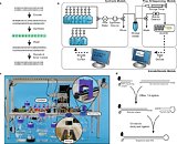
DNA, the most prominent genetic material, was successfully used as an end-to-end digital data storage medium. Nature reports that a team of biotechnologists led by Christopher N. Takahashi, Bichlien H. Nguyen, Karin Strauss & Luis Ceze with the University of Washington at Seattle, sponsored by DARPA and Microsoft, have succeeded in encoding and decoding digital information into DNA strands. With it, the team has developed an end-to-end DNA-based data storage device, which consists of an encoder that writes ones and zeroes into DNA sequences that are written into oligonucleotides; a liquid physical storage media in which the DNA is literally stored free from contamination and thermal hazards; and a decoder that consists of a nanopore sequencer.

The researchers have developed a protocol on how to convert 1s and 0s to A-G, C-T base-pairs, including error-correction. A 5-byte message "HELLO" was successfully encoded, stored, and decoded without data loss over a period of 21 hours. DNA-based storage unlocks innumerable possibilities. For starters, in the future, humans will be able to grow storage devices, store foreign information within their genome, and transmit digital information through plasmid agents such as purpose-built viruses. 007 writers must be rubbing their hands.

DARPA to Dedicate $100 million to EDA Projects Over the Next Five Years

EDA (Electronic Design Automation) is a quintessential part of modern silicon processor design - of any kind. Be it GPUs, CPUs, or SOCs, you can bet an electronic design tool has been applied somewhere in the process. These tools serve their function in various steps of silicon design, be it allowing for automated placement of components, signal routing, power optimization, and analyzing said designs with performance and bottleneck projections. It was rumored that Bulldozer was such a flawed architecture due to the overuse (and misuse) of EDA tools in its design; but mostly, usage of these tools is done in conjunction with engineers' hand-crafted, manually laid-out circuits.

In an effort to accelerate development and reduce cost of chip design (now approaching $500 million for a bleeding-edge SoC), two programs, IDEA (Intelligent Design of Electronic Assets) and POSH (Posh Open Source Hardware), involving 15 companies and more than 200 researchers, will receive $100 million in funding over the next five years. The IDEA is to create the equivalent of a silicon compiler, aimed at significantly lowering the barriers to design chips. POSH aims to create an open-source library of silicon blocks (that circuit designers can then mix and match according to their needs), and IDEA hopes to spawn a variety of open-source and commercial tools to automate testing of those blocks and actually grafting them into SoCs and finished products. Lower development costs means that lower-volume, specialized chips can now be developed more often, thus ushering a new era of specially-designed, fixed-function chips that are more efficient than mass-volume alternatives.

RISC-V Foundation Issues Statement on Spectre, Meltdown Exploits

Recent articles in the media have raised awareness around the processor security vulnerabilities named Meltdown and Spectre. These vulnerabilities are particularly troubling as they are not due to a bug in a particular processor implementation, but are a consequence of the widespread technique of speculative execution. Many generations of processors with different ISAs and from several different manufacturers are susceptible to the attacks, which exploit the fact that instructions speculatively executed on incorrectly predicted code paths can leave observable changes in micro-architectural state even though the instructions' architectural state changes will be undone once the branch prediction is found incorrect. No announced RISC-V silicon is susceptible, and the popular open-source RISC-V Rocket processor is unaffected as it does not perform memory accesses speculatively.

DARPA Believes the Future of Security to be in Additional Processing Hardware

DARPA seems to be taking to heart engineer and cyber-security experts' opinions that hardware-based security would be the best security. The Defense Advanced Research Agency (DARPA), which has appeared in every other sci-fi war movie, has started its System Security Integrated through Hardware and Firmware (SSITH) program, with an initial kick worth $3.6 million to the University of Michigan. The objective? To develop "unhackable" systems, with hardware-based security solutions that become impervious to most software exploits.

Electrical Engineering and Computer Science (EECS) of the University of Michigan Professor Todd Austin, lead researcher on the project, says his team's approach, currently code-named Morpheus, achieves hack-proof hardware by "changing the internal codes once a second". Austin likens Morpheus' defenses to requiring a would-be attacker to solve a new Rubik's Cube every second to crack the chip's security. In this way, the architecture should provide the maximum possible protection against intrusions, including hacks that exploit zero-day vulnerabilities, or those that cybersecurity experts have yet to discover. Morpheus thereby provides a future-proof solution, Austin said. "This race against ever more clever cyberintruders is never going to end if we keep designing our systems around gullible hardware that can be fooled in countless ways by software," SSITH program manager Linton Salmon of the Agency's Microsystems Technology Office.

Purdue University Develops Next-Gen, 3D Intrachip Cooling Technology

Researchers based on Purdue University have designed an intrachip cooling technology, which will likely pave the way for future generations of high performance 3D microprocessors. The research was part of a DARPA-funded commission for Purdue University's Birck Nanotechnology Center; a fundamental requirement stipulated by DARPA was the ability for this cooling system to handle chips generating 1 kW of heat per cm², more than 10x the amount current high-performance computers generate.

The new cooling system circulates an electrically insulated liquid coolant directly into electronic chips through an intricate series of tiny microchannels. This means that no longer will cooling systems be limited to the nowadays-employed conventional chip-cooling methods, which make use of finned metal plates called heat sinks. These are attached to computer chips to dissipate heat, but have a fundamental flaw: they do not remove heat efficiently enough for an emerging class of high-performance, 3D electronics, where too much heat hinders the performance of electronic chips or damages the tiny circuitry, especially in small "hot spots" that are located below the topmost layer of the chip.
Return to Keyword Browsing
Nov 23rd, 2024 18:43 EST change timezone

New Forum Posts

Popular Reviews

Controversial News Posts