Tuesday, October 31st 2017
Purdue University Develops Next-Gen, 3D Intrachip Cooling Technology
Researchers based on Purdue University have designed an intrachip cooling technology, which will likely pave the way for future generations of high performance 3D microprocessors. The research was part of a DARPA-funded commission for Purdue University's Birck Nanotechnology Center; a fundamental requirement stipulated by DARPA was the ability for this cooling system to handle chips generating 1 kW of heat per cm², more than 10x the amount current high-performance computers generate.
The new cooling system circulates an electrically insulated liquid coolant directly into electronic chips through an intricate series of tiny microchannels. This means that no longer will cooling systems be limited to the nowadays-employed conventional chip-cooling methods, which make use of finned metal plates called heat sinks. These are attached to computer chips to dissipate heat, but have a fundamental flaw: they do not remove heat efficiently enough for an emerging class of high-performance, 3D electronics, where too much heat hinders the performance of electronic chips or damages the tiny circuitry, especially in small "hot spots" that are located below the topmost layer of the chip.
 "You can pack only so much computing power into a single chip, so stacking chips on top of each other is one way of increasing performance," said Justin A. Weibel, a research associate professor in Purdue's School of Mechanical Engineering, and co-investigator on the project. "This presents a cooling challenge because if you have layers of many chips, normally each one of these would have its own system attached on top of it to draw out heat. As soon as you have even two chips stacked on top of each other the bottom one has to operate with significantly less power because it can't be cooled directly."
 Suresh V. Garimella, who is principal investigator for the project and the Goodson Distinguished Professor of Mechanical Engineering at Purdue University, added that "This transformative approach has great promise for use in radar electronics, as well as in high-performance supercomputers. In this paper, we have demonstrated the technology and the unprecedented performance it provides."
The system uses a commercial refrigerant called HFE-7100, a dielectric, or electrically insulating fluid, meaning it won't cause short circuits in the electronics. As the fluid circulates over the heat source, it boils inside the microchannels, somewhat like current vapor-chamber technology - but multiplied by X.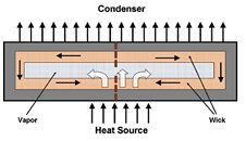 "Allowing the liquid to boil dramatically increases how much heat can be removed, compared to simply heating a liquid to below its boiling point," said Garimella. To increase efficiency and reduce pressure drops associated with long cooling channels that cover the length of the chip to be cooled, the team opted for a system of short, parallel channels, where a "hierarchical" manifold distributes the flow of coolant. "So, instead of a channel being 5,000 microns in length, we shorten it to 250 microns long," Garimella added. "The total length of the channel is the same, but it is now fed in discrete segments, and this prevents major pressure drops. So this represents a different paradigm."
Sources:
Purdue NewsRoom, via Hexus
The new cooling system circulates an electrically insulated liquid coolant directly into electronic chips through an intricate series of tiny microchannels. This means that no longer will cooling systems be limited to the nowadays-employed conventional chip-cooling methods, which make use of finned metal plates called heat sinks. These are attached to computer chips to dissipate heat, but have a fundamental flaw: they do not remove heat efficiently enough for an emerging class of high-performance, 3D electronics, where too much heat hinders the performance of electronic chips or damages the tiny circuitry, especially in small "hot spots" that are located below the topmost layer of the chip.


The system uses a commercial refrigerant called HFE-7100, a dielectric, or electrically insulating fluid, meaning it won't cause short circuits in the electronics. As the fluid circulates over the heat source, it boils inside the microchannels, somewhat like current vapor-chamber technology - but multiplied by X.

16 Comments on Purdue University Develops Next-Gen, 3D Intrachip Cooling Technology
I mean, if you have to take heat away 200W of heat from a chip the size of 5x5mm or same amount from the chip the size of 20x20mm, I think I don't have to further explain what we're facing here. We have coolers more than capable of dealing even with 16 core CPU's without much trouble, the problem is, they are really tiny. And AMD's approach of multiple dies and cores connected with Infinity Fabric is in a way having an edge over Intel's tiny monolithic designs. The heat output may be the same, but AMD has an easier way of managing it thanks to larger surface area.
www.eetimes.com/document.asp?doc_id=1168681
www.purdue.edu/newsroom/releases/2017/Q4/purdue-develops-intrachip-micro-cooling-system-for-high-performance-radar,-supercomputers---.html
Here is the article I quoted by Mark Lepedus:
BURLINGAME, Calif. -- IBM, Georgia Institute of Technology and Nanonexus presented a technology that involves 3D devices with integrated microchannel cooling.
In a paper, the companies claimed to have demonstrated a 3D silicon die with a density of 2500/cm2 -- and integrated with microchannel heat sinks.
With the technology, a microchanneled cooled processor at 3-GHz can operate at 83 Watts in 47 degree Celsius conditions, according to the paper. In comparison, an air cooled processor at 3-GHz operates at 102 Watts in 88 degree Celsius conditions, according to the paper.
The technology involves a 3D stacking technique called through-hole vias (TSVs). The problem with TSVs is to remove the heat in 3D structures, especially in microprocessor designs, said Deepak Sekar, an engineer at SanDisk Corp., who presented the paper at the IEEE 2008 International Interconnect Technology Conference (IITC) here this week.
''When two 100W/cm2 microprocessors are stacked on top of each other, for example, the net power density becomes 200W/cm2 and is beyond the heat removal limits of currently available air cooling technology,'' Sekar said in the paper.
The paper proposes the idea of fabricating TSVs on a wafer. First, a chip is fabricated. Second, the chip is etched to form the fluidic TSVs and microchannels. This is a two-step lithography process.
Third, the device is spin coated and polished with a sacrificial polymer material. Then, the polymer is spun-on, patterned and cured to form a cover for the TSVs and microchannels.
The microchannels are said to be 200-um tall and 150-um wide. The copper TSVs are 50-um in diameter. Silicon thickness is 400-um, while copper density is said to be 2500/cm2, according to the paper.
"Cooling fluid can be delivered to the 3D stack either using tubes on the back side of the 3D stack or using fluidic channels on the substrate,'' he said. ''The fluid is then delivered to the microchannel heat sinks on the back side of each chip in the 3D stack using fluidic through silicon vias and fluidic pipes.''
A two-chip 3D stack is said to show a junction-to-ambient thermal resistance of 0.24 degrees Celsius per Watt, according to the paper.
Chip scaling is showing no signs of hitting the wall--yet. But one alternative path--3D technology based on TSVs--continues to generate steam.
TSV technology took center stage at the IEEE 2008 International Interconnect Technology Conference (IITC) here this week. Georgia Institute of Technology, IBM, IMEC, Fraunhofer, Tohoku University, TSMC and others presented papers on TSV at IITC, although there is still no consensus just how the industry will bring the long-awaited technology into the mainstream.
Some more info on the topic published in 2014 : www.rit.edu/kgcoe/mechanical/taleme/Papers/Journal%20Papers/J141.pdf
But a monorail is, in fact, a train. So I dismiss It as a 200 years old tech.