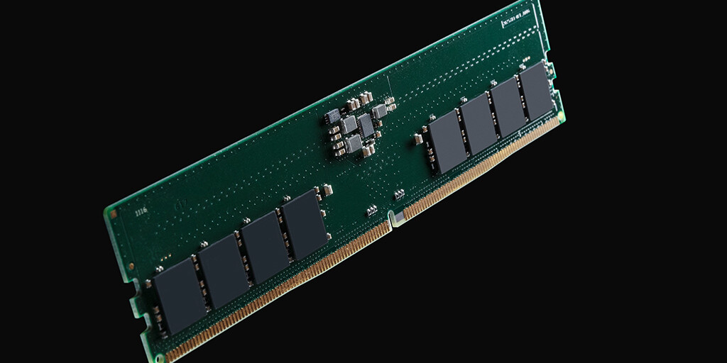
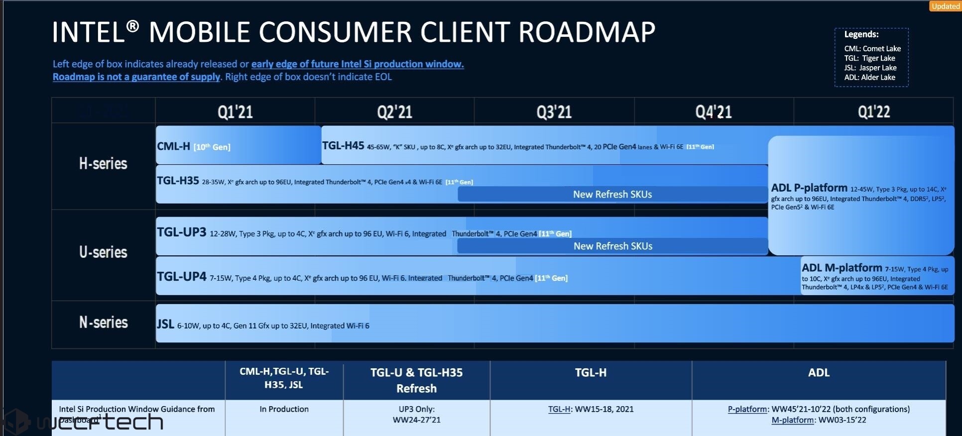
Kingston Technology First Third-Party Supplier to Receive Intel Platform Validation on DDR5 Memory
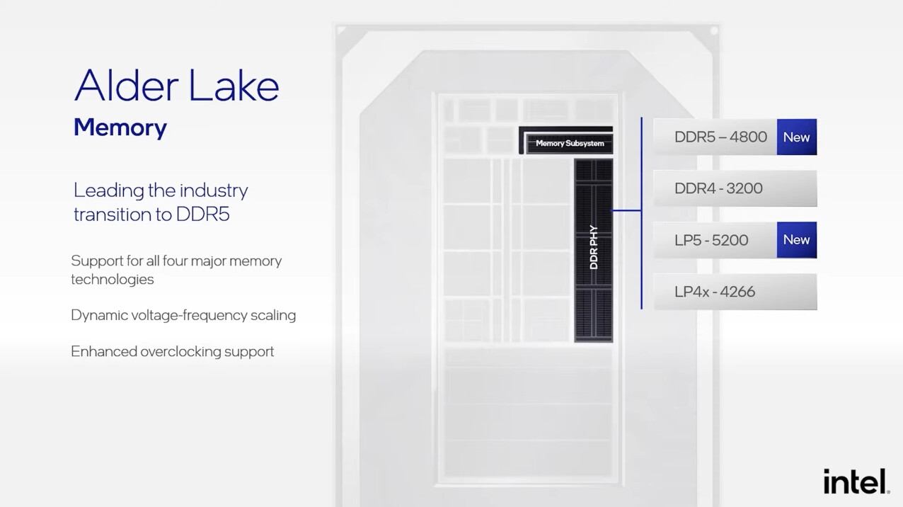
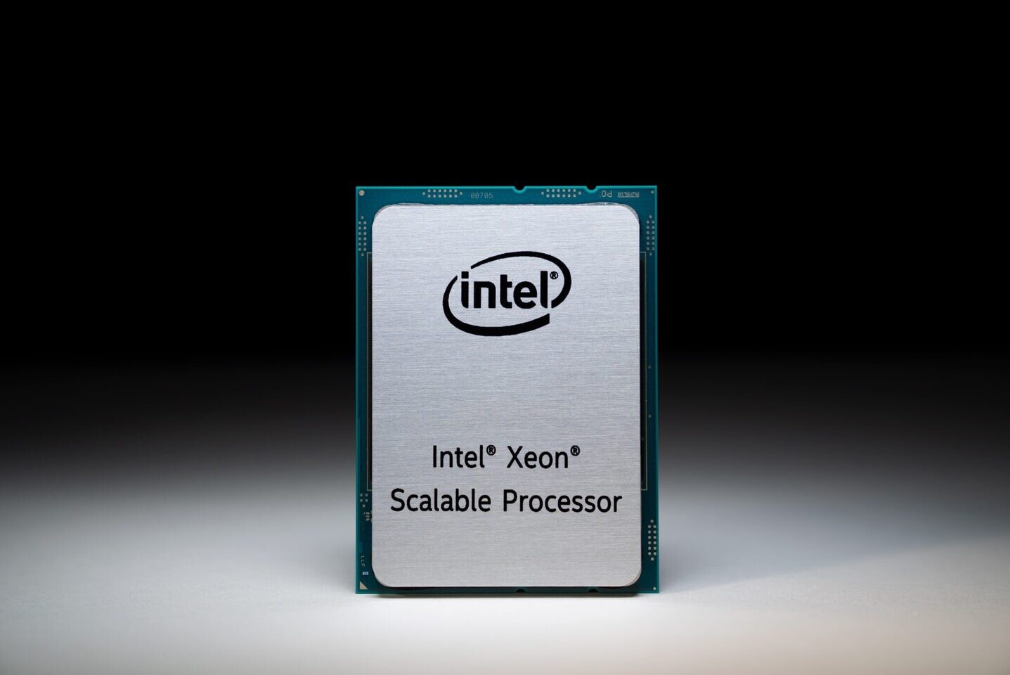
Kingston Technology Company, Inc., a world leader in memory products and technology solutions, today announced its forthcoming DDR5 UDIMMS have received Intel Platform Validation. This marks the first and arguably most important milestone in validating compatibility between Kingston DDR5 memory solutions and Intel platforms utilizing DDR5.
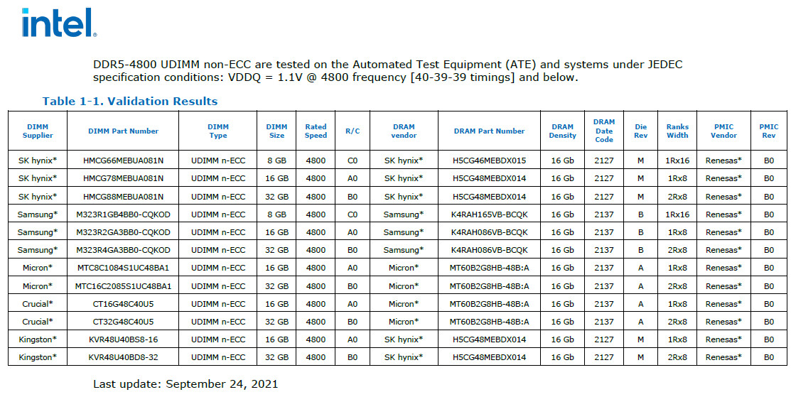
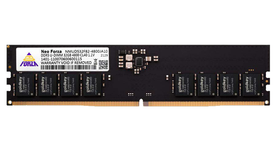
Kingston's introductory portfolio of DDR5 memory will be the first in a series of high performance, low to high capacity, multiple form factor solutions in support of DDR5 based platforms debuting over the next year. After developing the next generation of DDR memory, Kingston is providing over 10,000 DDR5 UDIMM samples to major motherboard manufacturers and technology partners in support of the platform launch. By supporting partners early, Kingston is doing its part to lay the foundation for a successful product launch.
Kingston's introductory portfolio of DDR5 memory will be the first in a series of high performance, low to high capacity, multiple form factor solutions in support of DDR5 based platforms debuting over the next year. After developing the next generation of DDR memory, Kingston is providing over 10,000 DDR5 UDIMM samples to major motherboard manufacturers and technology partners in support of the platform launch. By supporting partners early, Kingston is doing its part to lay the foundation for a successful product launch.