News Posts matching #DG2

Return to Keyword Browsing

Intel's Gaming Graphics Architecture, Xe-HPG, Now Sampling to Partners

Intel has begun sampling its Xe-HPG (High performance Gaming) products to ecosystem partners, which will allow them to verify performance, power, stability and board characteristics that are necessary variables in product development and launch. The information comes courtesy of Intel, who has updated its graphics product roadmap regarding DG2 sampling and for its Xe-HPC (High Performance Computing) products as well. Xe HPC products (codenamed Ponte Vecchio after a beautiful Florentine bridge) have now achieved power-on capabilities and are undergoing validation before subsequent steps in the hardware development workflow.

Intel DG2 GPU with 256 Execution Units Offers GTX 1050 Performance

We have been receiving several leaks for Intel's upcoming DG2 GPUs with a 256 Execution Unit model recently appearing on Geekbench paired with a 14-core Alder Lake mobile CPU. The Alder Lake mobile processor featured an integrated Xe GPU with 96 Execution Units which were also benchmarked. The 256 Execution Unit graphics card tested is likely derived from the mid-range DG2-384 GPU. The 96 EU DG2 iGPU featured a maximum frequency of 1.2 GHz while the 256 EU variant increased that to 1.4 GHz. The DG2-256 scored an OpenCL score of 18,450 points in the Geekbench 5 benchmark which places it at GTX 1050 performance level. The DG2-96 integrated GPU scored 6,500 points which is comparable to a GTX 460. While these performance numbers are low it is important to keep in mind that these are just early results from a mid-range mobile offering and Intel is planning to release cards with 512 Execution Units which should compete with the RTX 3070 Ti and 6700 XT.

Intel DG2 Graphics Card Leakers Suggest Performance Similar to NVIDIA RTX 3070 Ti, AMD RX 6700

Intel's foray into the discrete GPU market is inching ever closer, and with that diminishing time to market, leaks are getting more common. Renowned leaker TUM_APISAK has shared some performance numbers for Intel's upcoming DG2 graphics card, part of the company's Xe HPG (High Performance Gaming) architecture. In the leak, he also confirmed that Intel is working on a cut-down version of their top offering (which features 4,096 shading units spread across 512 EUs) in the form of a new SKU that offers 448 EUs and 3584 shading units running at 1.8 GHz. That is the actual chip whose relative performance was shared.

According to TUM_APISAK, users should expect the Intel DG2 448 EU graphics card to offer performance that's around the NVIDIA RTX 3070 (5% lower performance for the Intel part) and AMD's RX 6700 XT (8% lower performance for the Intel part). As for the performance of the full-fat 512 EU chip, another leaker, Moore's Law is Dead, expects its performance to fall very slightly lower than the performance offered by NVIDIA's RTX 3080 and AMD's RX 6800/6800 XT. The 512-EU DG2 should also feature higher Boost clocks up to 2.2 GHz. Intel's launch of their Xe HPG graphics architecture is expected to occur before the end of the year, likely starting with the highest performance/highest margin parts, trickling down the product stack through the beginning of 2022. Intel's launch should help in alleviating the lack of available graphics cards, whilst simultaneously breaking a duopoly market.

Intel's Raja Koduri Teases Xe-HPG (DG2) GPU with 512 Execution Units

Today, Mr. Raja Koduri, senior vice president, chief architect, and general manager of Architecture, Graphics, and Software at Intel, has teased Intel's upcoming Xe-HPG (DG2) gaming GPU on Twitter. Sharing a die shot of Intel's Xe-HPG design with 512 Execution Units (EUs), Mr. Koduri has highlighted the progress that the company is currently going through. The Xe-HPG will represent the company's efforts of going into a very competitive discrete GPU market, dominated by a duopoly of AMD and NVIDIA. The Xe-HPG design pictured below is representative of a maxed-out SKU with 512 EUs, translating into 4096 shading units. This model is expected to be paired with 16 GB of GDDR6 memory.

"From jittery journeys to buttery smooth" - it is quoted in a Tweet of Mr. Koduri. This doubles down on the efforts Intel is putting into creating a GPU and the difficulties that the company is facing. It is also noted that there remains a lot of work in form of driver coding and a lot of game optimizations, which are very important for the new GPU. You can check out the complete Tweet below.
Raja KoduriXe-HPG (DG2) real candy - very productive time at the Folsom lab couple of weeks ago. "From jittery journeys to buttery smooth" said @rogerdchandler - lots of game and driver optimization work ahead for @gfxlisa's software team. They are all very excited..and a little scared:)
Intel Xe-HPG (DG2) Die Picture

Intel Xe-HPG DG2 GPU Specifications Leak, First GPUs are Coming in H2 2021 in Alder Lake-P Laptops

Yesterday, we got information that Intel's upcoming DG2 discrete graphics card is "right around the corner". That means that we are inching closer to the launch of Intel's discrete GPU offerings, and we are going to get another major player in the current GPU market duopoly. Today, however, we are in luck because Igor from Igor's LAB has managed to get ahold of the specifications of Intel's Xe-HPG DG2 graphics card. For starters, it is important to note that DG2 GPU will first come to laptops later this year. More precisely, laptops powered by Alder Lake-P processors will get paired with DG2 discrete GPU in the second half of 2021. The CPU and GPU will connect using the PCIe 4.0 x12 link as shown in the diagram below, where the GPU is paired with the Tiger Lake-H processor. The GPU has its subsystem that handles the IO as well.

Intel Xe DG2 Graphics Card "Right Around the Corner:" Game Dev Relations Engineer

A senior game developer relations engineer at Intel, Pete Brubaker, Tweeted late Wednesday that the company's DG2 discrete graphics card is "right around the corner," and that "it's about to get exciting." Brubaker's Tweet comes as the company is looking to recruit more engineers to work with its developer relations, the team that interfaces with game devs to optimize their engines and games for Intel's graphics architectures.

While the DG1, which was productized as the Iris Xe MAX graphics card, was essentially an iGPU-on-a-stick, the DG2 should spark a lot more interest. Based on a third-party foundry process, the DG2 is the first client graphics product based on the Xe HPG (high performance gaming) graphics architecture, and allegedly crams up to 512 execution units or 4,096 unified shaders—a 4.3x gain over the Iris Xe MAX. It's also rumored to ship with up to 16 GB of GDDR6 memory across a 256-bit wide memory bus. Whether it features DirectX 12 Ultimate features or not, remains to be seen, but it's becoming clear that Intel wants a crack at the high-volume e-sports market, with a product that's fast enough for competitive e-sports gaming, and capable of AAA.

Intel Xe-HPG DG2 GPU Engineering Sample Pictured

We have recently received pictures of any early engineering sample of Intel's upcoming DG2 GPU from YouTuber Moore's Law is Dead. The card features 512 Execution Units and will be the flagship model for Intel's upcoming Xe-HPG lineup reportedly targeting performance between the RTX 3070 and RTX 3080. The final product is rumored to feature a base clock of 2.2 GHz along with 16 GB GDDR6 memory and a 256-bit bus. The sample has a TDP of 275 W with 8 + 6 pin power connectors up from original targets of 225 W - 250 W.

The report also notes that Intel is still deciding between three cooler designs with the finished card potentially featuring a white shroud. Intel also appears to be working on a NVIDIA DLSS/AMD FidelityFX Super Resolution competitor codenamed XeSS which confirms support for hardware-accelerated raytracing and resolution upscaling tech. The card is unlikely to launch until Q4 2021 with wider availability in 2022, lower end 128 EU, and 256 EU cards will follow shortly afterward. The full report can be viewed below.

New Intel DG2 HPG GPU Surface, Could Power a Family of Products

It appears that Intel's DG2 refers to a number of HPG (High Performance Graphics) products within the same family, with rumors surfacing around a possible total of six different graphics products based on the company's latest high performance graphics architecture - and its debut on the high performance discrete market. It's been confirmed that Intel's DG2 products will not be manufactured in-house, via Intel's 10 nm SuperFin technology, but with recourse to foundry partner TSMC's 6 nm fabrication technology.

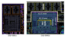
It seems that DG2 is currently slated for launch based on three different chip configurations: the first is the DG2 512EU, which will power the highest-performance, 4096 shading unit, 8 GB / 16 GB GDDR6 and 192-bit bus graphics card. Another chip is the DG12 384EU, estimated to come in at ~190 mm², available in three different shading unit configurations: 3072 shading units, with an accompanying 6/12 GB of GDDR6 memory and 192-bit bus; 2048 shading units, which reduces allotted memory to 4/8 GB configurations and a 128-bit memory bus; and finally, the further cut-down 1536 shading unit configuration, with a maximum of 4 GB of GDDR6 memory over the same 128-bit bus. The final (current) chip in the DG2 family is the DG2 128EU, with both 128EU and 96EU configurations (1024 and 768 shading units, respectively) carrying 4 GB VRAM over a pretty tight 64-bit bus. We'll see if these leaks actually materialize into final Intel products, and if these design choices are the possible best, considering Intel's technology, so as to assail the two-player party that is the discrete, high performance graphics market.

Intel Xe-HPG to be Built on TSMC N7: Report

Intel's first discrete gaming graphics card based on the Xe-HPG graphics architecture, will be built on a TSMC 7 nanometer silicon fabrication node, according to a Reuters report citing sources "familiar with the matter." The first such discrete GPU is being referred to internally by Intel as the DG2. Recent reports suggest that Intel will give the DG2 formidable specs, such as 4,096 unified shaders across 512 execution units, and 8 GB of GDDR6 video memory. Back in 2020, the company launched the DG1 under the Intel Iris Xe MAX marketing name, targeting only the mobile discrete GPU market. The DG1 has entry-level specs, with which Intel is eyeing the same pie as NVIDIA's fast-moving GeForce MX series mobile GPUs. Interestingly, the other major client of TSMC-N7 following Apple's transition to N5, is Intel's rival AMD.

Intel Xe-HP "NEO Graphics" GPU with 512 EUs Spotted

Intel is preparing to flood the market with its Xe GPU lineup, covering the entire vector from low-end to high-end consumer graphics cards. Just a few days ago, the company has announced its Iris Xe MAX GPU, the first discrete GPU from Intel, aimed at 1080p gamer and content creators. However, that seems to be only the beginning of Intel's GPU plan and just a small piece of the entire lineup. Next year, the company is expected to launch two GPU families - Xe-HP and Xe-HPG. With the former being a data-centric GPU codenamed Arctic Sound, and the latter being a gaming-oriented GPU called DG2. Today, thanks to the GeekBench listing, we have some information on the Xe-HP GPU.

Being listed with 512 EUs (Execution Units), translating into 4096 shading units, the GPU is reportedly a Xe-HP variant codenamed "NEO Graphics". This is not the first time that the NEO graphics has been mentioned. Intel has called a processor Neo graphics before, on its Architecture day when the company was demonstrating the FP32 performance. The new GeekBench leak shows the GPU running at 1.15 GHz clock speed, where at the Architecture day the same GPU ran at 1.3 GHz frequency, indicating that this is only an engineering sample. The GPU ran the GeekBench'es OpenCL test and scored very low 25,475 points. Compared to NVIDIA's GeForce RTX 3070 GPU that scored 140,484, the Intel GPU is at least four times slower. That is possibly due to the non-optimization of the benchmark, which could greatly improve in the future. In the first picture below, this Xe-HP GPU would represent the single-tile design.

Intel Xe-HPG DG2 GPU is in the Labs

In its Q3 earnings, Intel disclosed that it is now shipping Intel's first discrete GPU - DG1. Codenamed Intel Iris Xe MAX, the GPU is set to arrive in ultraportable laptops and designs. It is based on Xe-LP design, which is Intel's GPU configuration for iGPUs and low-power models. However, to satisfy the needs of gamers, Intel will not be good with just this GPU configuration. The company would need something faster and ore power-hungry to power the highest framerates and highest resolutions. Enter the world of Xe-HPG DG2 GPU. Made for gamers, it features all the hardware-enabled features you would expect in such a GPU, like raytracing, etc. This GPU is manufactured outside Intel's fabs, most likely at TSMC's facilities. Right now, this GPU is in the alpha phase and is booting in Intel's labs, meaning that the final silicon is just a few months away.

Intel DG2 Discrete Xe Graphics Block Diagram Surfaces

New details have leaked on Intel's upcoming DG2 graphics accelerator, which could help shed some light on what exactly can be expected from Intel's foray into the discrete graphics department. For one, a product listing shows an Intel DG2 graphic accelerator being paired with 8 GB of GDDR6 memory and a Tiger Lake-H CPU (45 W version with 8 cores, which should carry only 32 EUs in integrated graphics hardware). This 8 GB of GDDR6 detail is interesting, as it points towards a 256-bit memory bus - one that is expected to be paired with the 512 EU version of Intel's DG2 (remember that a 384 EU version is also expected, but that one carries only 6 GB of GDDR6, which most likely means a 192-bit bus.

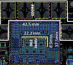
Videocardz says they have received an image for the block diagram on Intel's DG2, pointing towards a 189 mm² die area for the 384 EU version. Looking at component density, it seems that this particular diagram may refer to an MXM design, commonly employed as a discrete notebook solution. 6 total GDDR6 chips are seen in the diagram, thus pointing towards a memory density of 6 GB and the aforementioned 192-bit bus. Other specs that have turned up in the meantime point towards a USB-C interface being available for the DG2, which could either point towards a Thunderbolt 4-supporting design, or something like Virtual Link.
Return to Keyword Browsing
Dec 18th, 2024 06:04 EST change timezone

New Forum Posts

Popular Reviews

Controversial News Posts