During GTC 2025, NVIDIA unveiled the
professional (PRO) side of its "Blackwell" GPU line—headlined by a
monstrous GDDR7 96 GB option, that unleashes the full potential of their
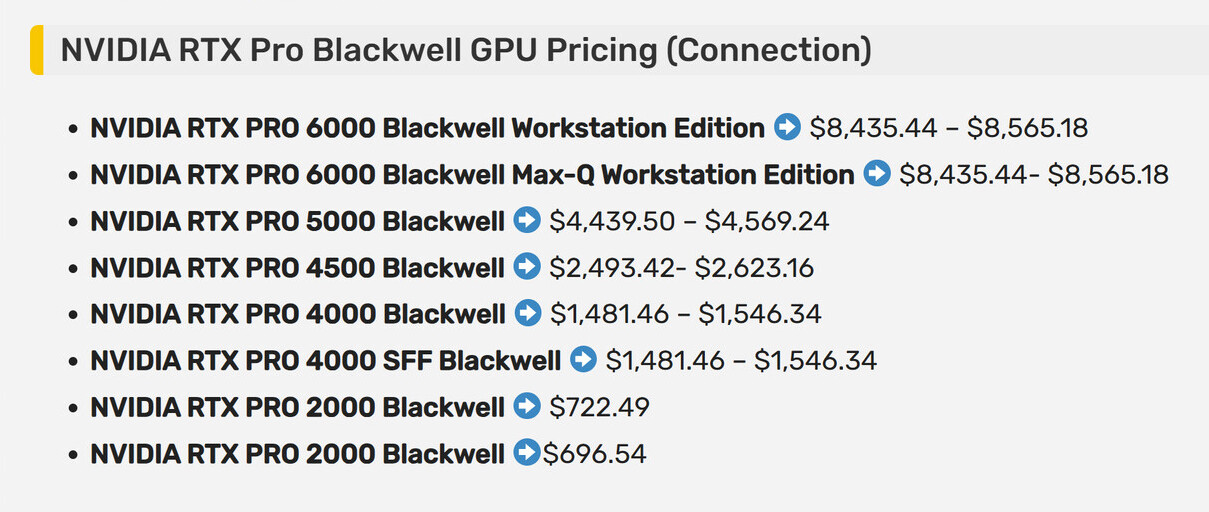
GB202 die. Industry watchdogs anticipated sky-high pricing, as befits such a potent specification sheet/feature set. As reported by VideoCardz over the past weekend, a North American enterprise PC hardware store—Connection—has populated its webshop with several of Team Green's brand-new RTX PRO Blackwell Series SKUs. The publication received tip-offs from a portion of its readership; including some well-heeled individuals who have already claimed pre-orders. Starting off, the investigation highlighted upper crust offerings: "the flagship model, called the RTX PRO 6000 with 96 GB of VRAM, will launch at $8435 (bulk) to $8565 (box), and this price seemingly applies to both models: the Workstation Edition and a
sub-variant called Max-Q. Both are equipped with the same specs, but the latter is capped at 300 W TDP while retaining 88% of the Al performance, claimed NVIDIA."
Connection has removed its RTX PRO 6000 Blackwell and RTX PRO 6000 Blackwell Max-Q product pages, but the rest of Team Green's professional stack is still visible (see relevant screenshot below). The
RTX PRO 5000 Blackwell 48 GB card is priced at $4569.24 (or $4439.50 for bulk). The cheapest offering is a $696.54 RTX PRO 2000 Blackwell 8 GB model. Officially, NVIDIA and its main professional series board partner—PNY—only
revealed 4500, 5000 and 6000 product tiers. VideoCardz put a spotlight on some of these unannounced options, including: "the
RTX 4000 non-SFF version, while this retailer has six listings for such SKUs (two SFF and two non-SFF, both in bulk and box variants). Presumably, this would suggest that NVIDIA may launch a non-SFF version later. However, the company didn't put 'SFF' in the official card's name, so perhaps this information is no longer valid, and there's only one model." According to a GDM/Hermitage AkiHabara Japan
press release, a local reseller—Elsa—is preparing NVIDIA RTX PRO 6000 Blackwell Workstation Edition and RTX PRO 6000 Blackwell Max-Q Workstation Edition stock for scheduled release "in May 2025, while the other models are scheduled for release around summer." Additionally, another retailer (ASK Co., Ltd.): "has stated that the price and release date are subject to inquiry."