News Posts matching #GK104

Return to Keyword Browsing

Raijintek Rolls Out Morpheus Core Edition VGA Cooler

Raijintek announced the Morpheus Core Edition, a matte-black variant of its popular universal VGA cooler. Armed with a large monolithic aluminium fin stack of 129 fins, the cooler features a nickel-plated copper base, with mirror finish. Six 6 mm thick nickel-plated copper heat pipes with dark / gunmetal finish, spread heat across the fin stack. The cooler can hold on to two common 120 mm fans for ventilation. It can soak up thermal loads of up to 360W, making it fit for a variety of feisty high-end GPUs, such as the GeForce GTX 780 Ti, the Radeon R9 290X, and other GPUs based on the GK104, GM204, and "Pitcairn" silicons. Heatsinks for VRM, and 24 heatsinks for memory chips, come included. Raijintek didn't announce pricing or availability details.
A video presentation follows.

Even More GeForce GTX 980 and GM204 Specs Tumble Out

Ahead of its launch later this week, even more details of NVIDIA's upcoming GeForce GTX 980, and the 28 nm "GM204" silicon it's based on, tumbled out. To begin with, the GM204 silicon is confirmed to be built on the 28 nm silicon fab process. The chip bigger than that of the GK104, with a die area of 398 mm², yet smaller than the GK110, which measures 581 mm². Its transistor count is 5.2 billion, about 2 billion more than the GK104.

The component hierarchy of GM204 is similar to that of the GM107 silicon, on which the GTX 750 Ti is based. The GPU features a 256-bit wide GDDR5 memory interface, and PCI-Express 3.0 x16 bus. The GigaThread Engine dispatches workload between four graphics processing clusters (GPCs), the basic subunit. Each GPC has a common raster engine shared between four streaming multiprocessors Maxwell (SMMs), which each hold 128 CUDA cores. The total CUDA core count is hence 2,048. The L2 cache has been quadrupled over GK104. The chip features 2 MB of it, compared to 512 KB on its predecessor. The GM204 features 64 ROPs, double that of the GK104, and should hence come with a strong geometry processing muscle. The chip features a revolutionary new 3-bit delta color compression technology that makes the most of the limited memory bus width of this chip.

Galaxy GeForce GTX 970 Pictured, Specs Confirmed, Early Benchmarks Surface

Here are some of the first pictures of an AIC partner branded NVIDIA GeForce GTX 970 graphics card, the Galaxy GTX 970 GC. Spotted across Chinese PC enthusiast forums and social networks, the latest set of leaks cover not just pictures of what the GTX 970 looks like, but also what's under its hood. To begin with, Galaxy's card appears to be built for the high-end market segment. A meaty twin-fan aluminium fin-stack heatsink, coupled by a spacey backplate cover a signature Galaxy blue PCB, holding NVIDIA's new GTX 970 GPU, and 4 GB of GDDR5 memory. The card appears to feature a high-grade VRM that draws power from a combination of 8-pin and 6-pin PCIe power connectors.

NVIDIA Tweaking GeForce GTX 770 Price to Compete with R9 285

NVIDIA's response to AMD Radeon R9 285 isn't major (a new product launch). The company believes it already has the products out there to take on it. The company is likely working with add-in card partners, and retailers, to tweak pricing of its performance-segment GeForce GTX 770 2GB, bringing its price around the US $275 mark, $25 more than the cheapest R9 285, and roughly the same price as factory-overclocked ones. Its pricing is down from the $325 point it was hovering over.

The GTX 770 costs roughly the same as the GTX 760, for NVIDIA to sell, with the former only imposing slightly higher VRM requirements. Our tests show that the GTX 770 still ends up with better energy efficiency figures than the R9 285. Based on the 28 nm "GK104" silicon, the GTX 770 packs 1,536 CUDA cores, 128 TMUs, 32 ROPs, and a 256-bit wide GDDR5 memory interface.

AMD Radeon R9 285 Launch Date Revealed

AMD is set to launch its new performance-segment graphics card, the Radeon R9 285, on the 2nd September, 2014. Ahead of its launch, the company is expected to tease the card at its August 23rd press-event, celebrating 30 years of graphics and gaming. On that day, AMD will share "partial" details of the card.

The R9 285 is based on AMD's swanky new 28 nm "Tonga" silicon, which is being drummed up to be AMD's best answer to NVIDIA's GK104. The chip offers performance rivaling "Tahiti," at the power consumption of GK104. The R9 285 is being designed to offer performance roughly that of the Radeon R9 280, at energy-efficiency, and pricing to drop lead on NVIDIA's GeForce GTX 760. A month later, presumably in early October, the company plans to launch the faster R9 285X, offering performance comparable (if not higher than) the R9 280X, at the energy-efficiency levels of GTX 770. "Tonga" physically features 2,048 Graphics CoreNext 1.1 stream processors, 128 TMUs, 32 ROPs, and a 256-bit wide GDDR5 memory interface, which will hold 2 GB or 4 GB of memory.

NVIDIA to Launch GeForce GTX 880 in September

NVIDIA is expected to unveil its next generation high-end graphics card, the GeForce GTX 880, in September 2014. The company could tease its upcoming products at Gamescom. The company is reportedly holding a huge media event in California this September, where it's widely expected to discuss high-end graphics cards based on the "Maxwell" architecture. Much like AMD's Hawaii press event that predated actual launch of its R9 290 series by several weeks; NVIDIA's event is expected to be a paper-launch of one or more graphics cards based on its GM204 silicon, with market availability expected in time for Holiday 2014 sales.

The GM204 is expected to be NVIDIA's next workhorse chip, which will be marketed as high-end in the GeForce GTX 800 series, and performance-segment in its following GTX 900 series; much like how the company milked its "Kepler" based GK104 across two series. It's expected to be built on the existing 28 nm process, although one cannot rule out an optical shrink to 20 nm later (like NVIDIA shrunk the G92 from 65 nm to 55 nm). The GTX 880 reportedly features around 3,200 CUDA cores, and 4 GB of GDDR5 memory.

GeForce GTX 880 ES Intercepted En Route Testing Lab, Features 8 GB Memory?

An engineering sample (ES) of the GeForce GTX 880 was intercepted on its way from a factory in China, to NVIDIA's development center in India, where it will probably undergo testing and further development. The shipping manifest of the courier ferrying NVIDIA's precious package was sniffed out by the Chinese press. NVIDIA was rather descriptive about the ES, in its shipping declaration. Buzzwords include "GM204" and "8 GB GDDR5," hinting at what could two of the most important items on its specs sheet. GM204 is a successor of GK104, and is rumored to feature 3,200 CUDA cores, among other things, including a 256-bit wide memory bus. If NVIDIA is cramming 8 GB onto the card, it must be using some very high density memory chips. The manifest also declares its market value at around 47,000 Indian Rupees. It may convert to US $780, but adding all taxes and local markups, 47,000 INR is usually where $500-ish graphics cards end up in the Indian market. The R9 290X, for example, is going for that much.

Leadtek Announces GeForce GTX 760 4GB Hurricane

Leadtek announced the WinFast GeForce GTX 760 Hurricane graphics card with 4 GB of memory (model: WFGTX760-4GD5DF3OC), in what could be among the first of many upcoming GTX 760 graphics cards to ship with double the standard memory amount, to meet with Battlefield 4 recommended system requirements that mandate at least 3 GB of graphics memory. Leadtek's card features a compact dual-slot aluminium fin-stack heatsink that uses four 8 mm-thick nickel-plated copper heat pipes to convey heat from the GPU to two fin-stacks; which are ventilated by a pair of 74 mm fans. Apart from 4 GB of memory, the card ships with factory overclocked speeds of 1111 MHz core (compared to 980 MHz reference), and 6280 MHz memory (compared to 6008 MHz reference, GDDR5-effective). Based on the 28 nm GK104 silicon, the GeForce GTX 760 features 1,152 CUDA cores, and a 256-bit wide memory interface.

NVIDIA Prepares Two New Sub-$250 SKUs, Price Cuts

With AMD detailing its Radeon R9 and R7 series, especially at some very attractive sub-$299 price-points for the most part, there are jitters being felt at NVIDIA. The company is expected to unveil one or two new sub-$250 GeForce GTX SKUs around mid-October, 2013. The company is also expected to introduce price-cuts across its entire lineup, to make it competitive with AMD's. NVIDIA could tap into its existing GK104 and GK106 silicons to carve out the two new SKUs ranging between $149.99 and $249.99. The idea here would be to topple Radeon R9 270X. Price-cuts could be directed at the likes of GeForce GTX 760 and GTX 770, to make them competitive with the Radeon R9 280X, while in anticipation of the $599 pricing of the R9 290X, NVIDIA could rethink pricing of its $650 GeForce GTX 780, and $1000 GTX TITAN.

NVIDIA GeForce GTX 750 Ti Detailed?

How far can you strip down a GK104? Very far. Reports from the Chinese press and the whirring rumor mill there speaks of a new mid-range graphics card SKU taking shape at NVIDIA, named GeForce GTX 750 Ti, which is being designed to succeed the GeForce GTX 650 Ti Boost, outperform the GeForce GTX 660, and become NVIDIA's posterboy for this year's AAA shooter releases - Call of Duty: Ghosts, and Battlefield 4, when the company expects a tiny spike in GPU sales.

Based on the same G92 GK104 silicon as several other 600- and 700-series GeForce GTX products, the GTX 750 Ti will be configured a notch above the GK106-based GeForce GTX 660. To begin with, it's expected to feature 960 CUDA cores, a notch below the 1152 cores on the GeForce GTX 760. It has the same 80 TMUs as the GTX 660, but 32 ROPs and a 256-bit wide memory interface (compared to 24 ROPs and 192-bit on the GTX 660). Clock speeds are expected to be higher, too, at 1033 MHz core, 1098 MHz GPU Boost, and 6.00 GHz (GDDR5-effective) memory. There's no clarity on when exactly NVIDIA plans to launch the SKU, but we expect that to happen before AMD's late-September high-end extravaganza.

Galaxy Rolls Out GeForce GTX 760 Mini

Galaxy rolled out a minimalist, and compact GeForce GTX 760 graphics card, the GTX 760 Mini (model: GF PGTX760-OC/2GD5 MINI). It features a compact GK104 PCB that's just 19.3 cm long, and a cooler that isn't over the top for the chip. Despite that, a small factory-overclock is on offer. The GPU is clocked at 1019 MHz (vs. 980 MHz reference), and GPU Boost at 1084 MHz (vs. 1033 MHz reference). The memory is untouched, at 6008 MHz (GDDR5-effective). The cooler uses a dense aluminum fin stack, to which heat is fed by three 8 mm-thick copper heat pipes, and which is ventilated by a pair of 70 mm fans. Based on the 28 nm GK104 silicon, the GeForce GTX 760 features 1,152 CUDA cores, and a 256-bit wide GDDR5 memory interface.

ELSA Announces GeForce GTX 760 SAC Graphics Card

ELSA announced its non-reference GeForce GTX 760 offering, the GTX 760 SAC (silent air-cooling). Based entirely on Inno3D's iChill design, the card features a blue-colored non-reference design PCB, and a cooling solution that's easy to clean. It uses a conventional aluminum fin-stack design, covered by an easy-to-remove die-cast metal shroud, on which its two 70 mm fans are suspected. The shroud can be detached by simply turning a few thumb-screws, letting you clean the fans and heatsink. The GTX 760 SAC features NVIDIA-reference clock speeds of 980 MHz core, 1033 MHz GPU Boost, and 6.00 GHz memory. Based on the 28 nm GK104 silicon, the GeForce GTX 760 packs 1,152 CUDA cores, 96 TMUs, 32 ROPs, and a 256-bit wide GDDR5 memory interface, holding 2 GB of memory. ELSA is including a 1-week's subscription to ArcheAge, a Japanese MMO.

NVIDIA Announces the GeForce GTX 760 Graphics Card

NVIDIA launched its newest performance segment graphics card, the GeForce GTX 760. Designed to succeed GeForce GTX 660, it displaces the GeForce GTX 660 Ti from the product stack. Based on the same GK104 silicon as GeForce GTX 770, it features 1,152 CUDA cores, 96 TMUs, 32 ROPs, and a 256-bit wide GDDR5 memory interface, holding 2 GB of memory. NVIDIA partners are free to come up with factory-overclocked, non-reference design, and 4 GB variants, from day one.

The GeForce GTX 760 offers clock speeds of 980 MHz core, 1033 MHz GPU Boost, and 6.00 GHz memory (192 GB/s). It features GPU Boost 2.0, which rewards better cooling, with better sustenance of GPU Boost clock states. Interestingly, NVIDIA let it support 3-way and 4-way SLI, which is a first for this market segment. The GTX 760 starts at a pleasantly surprising US $249.99, available starting today. Factory-overclocked 2 GB cards should be priced up to $300, while 4 GB variants should exceed it.
TechPowerUp reviewed the following GeForce GTX 760 graphics cards for you today:

NVIDIA GTX 760 (reference design) | ASUS GTX 760 DirectCU II OC | EVGA GTX 760 SC with ACX | GIGABYTE GTX 760 WindForce OC | MSI GTX 760 GAMING | Palit GTX 760 JetStream

GeForce GTX 760 Last 700 Series SKU for 2013?

NVIDIA's upcoming GeForce GTX 760 could be the company's last GTX 700 series retail desktop SKU, at least for this year. A leaked slide by the company lays out how this year's three new GTX 700 series SKUs pretty much seal the product stack. It reveals that GeForce GTX TITAN will remain NVIDIA's flagship graphics card throughout the year. The thousand-dollar single-GPU card is based on the GK110 silicon, with 2,688 CUDA cores, and 6 GB of memory. The GeForce GTX 780, introduced this March, replaces the GeForce GTX 680 on the product-stack, even at its much higher launch price of $650, compared to its predecessor's $500. The GTX 780 has no competition from AMD at its price-point.

The slide also reveals that the GeForce GTX 770, which was launched late last month, will replace the GeForce GTX 670 from the stack. Based on the GK104 silicon, it features 1,536 CUDA cores, and 2 to 4 GB of memory. Given that it has a lot in common with the GeForce GTX 680, albeit with higher clock speeds, GPU Boost 2.0, its $400 pricing surprised us. The GeForce GTX 770 outperforms AMD's HD 7970 GHz Edition, and is generally priced on-par. The only definitively faster AMD card is the $1100 HD 7990 "Malta," which makes the GTX 770 the king of its segment.

ASUS GeForce GTX 760 DirectCU II OC Listed

European price-aggregator Geizhals.at sniffed out at least two retailers listing the upcoming ASUS GeForce GTX 760 DirectCU II OC graphics card. The card is priced at 316.5€ on average, including VAT and shipping; and 264€ excluding them. While the card itself isn't pictured by either store, specifications posted by Geizhals appear to check out with Monday's leaks. The card is based on a 28 nm GK104 silicon, with 1,152 CUDA cores, 96 TMUs, 32 ROPs, and a 256-bit wide memory interface holding 2 GB of memory. The way Geizhals describes it, the card features a dual-slot DirectCU II cooler. We don't expect it to look much different from the one that cools DirectCU II versions of GTX 660 Ti or GTX 670. The 264€ pre-VAT pricing of this non-reference design, factory-overclocked card suggests that most GTX 760 cards should be priced in the neighborhood of US $250 to $300.

NVIDIA GeForce GTX 760 Specifications Redux

There are many theories doing rounds about the specifications of NVIDIA's upcoming performance-segment GPU, the GeForce GTX 760. One states that it's largely similar to the GeForce GTX 660 Ti from previous-generation, with higher clock speeds, possibly 7.00 GHz memory, and GPU Boost; while another suggests a completely new core-configuration. According to a GPU-Z screenshot leaked by a ChipHell community member, NVIDIA is attempting to give the GeForce GTX 660 a successor, rather than merely retrofitting the GTX 660 Ti.

According to leaks that surfaced on ChipHell, NVIDIA is configuring a GK104 GPU with just three out of four GPC (graphics processing clusters) enabled, while keeping the memory and raster operations untouched. This approach would give the chip 1,152 CUDA cores, 96 TMUs, 32 ROPs, and a 256-bit wide GDDR5 memory interface. The card in the GPU-Z screenshot features 1072 MHz core, 1111 MHz GPU Boost, and 7.00 GHz memory.

MSI Launches a Pair of GeForce GTX 770 Graphics Cards

MSI kicked off its GeForce GTX 770 lineup with two models, the GTX 770 Gaming Series, and the GTX 770 Lightning, both of which are factory-overclocked models. The Gaming Series card (model: N770TF/2GD5 OC) ships with 1098 MHz core, 1150 MHz GPU Boost, and 7010 MHz memory; while the Lightning (model: N770Lightning), ships with 1150 MHz core, 1202 MHz GPU Boost, and the same 7010 MHz memory. Both cards come with 2 GB of GDDR5 memory.

The GTX 770 Gaming Series OC features a new generation TwinFrozr cooling solution with large 100 mm fans, and the sexy red+black color scheme, paired with the Gaming Series "dragon" emblem. The GTX 770 Lightning, on the other hand, features the same TwinFrozr IV cooling solution we find on the GTX 680 Lightning. Based on the 28 nm GK104 silicon, the GeForce GTX 770 packs 1536 CUDA cores, 128 TMUs, 32 ROPs, and a 256-bit wide GDDR5 memory interface. MSI didn't reveal pricing or availability information.

NVIDIA Announces GeForce GTX 770 Performance Graphics Card

NVIDIA launched the business-end of its GeForce GTX 700 series, launching the GeForce GTX 770. Tough to make apart from GeForce GTX 780 and GeForce GTX TITAN visually, the GTX 770 is based on the 28 nm GK104 silicon, configured similarly to the GeForce GTX 680 from the previous generation, albeit with higher clock speeds, GPU Boost 2.0, and a stronger VRM to sustain those higher clock speeds. The card ships with 1046 MHz core, 1085 MHz GPU Boost, and a blistering 7010 MHz (GDDR5-effective) memory. It features 2 GB of memory, 4 GB variants could launch soon.

The GeForce GTX 770 packs 1,536 CUDA cores, 128 TMUs, and 32 ROPs, and a 256-bit wide GDDR5 memory interface. At its given memory speeds, it could belt out 224 GB/s of memory bandwidth. To support these higher clock speeds, the card draws power from a combination of 8-pin and 6-pin PCIe power connectors. Display outputs include a pair of DVI, an HDMI, and DisplayPort. The card can pair with three more of its kind, for 4-way SLI. As predicted, the GeForce GTX 770 starts at US $399. NVIDIA's partners could come out with custom-design cards from day-one.

GeForce GTX 770 Specifications Leaked, Could Surprise with Pricing

NVIDIA's GeForce GTX 770 could end up being the product we expected it to be specifications-wise, but could surprise with pricing, according to retailers in Tokyo's Akihabara electronics shopping district. On paper, the GTX 770 is virtually identical to the GeForce GTX 680, albeit with higher core clocks, and a record memory frequency. The chip features 1046 MHz core, 1085 MHz of GPU Boost, and a staggering 7.00 GHz (1750 MHz actual) memory.

If true, the GTX 770 should be the highest-clocked GPU ever built. These clocks bolster the same 14-month old GK104 silicon we're all too familiar with. To support these clocks, the card draws power from a combination of 6-pin and 8-pin power connectors, and features a rated TDP of 230W. The card features a cooling solution identical to the GeForce GTX 780 and GTX TITAN, which should make it an attractive buy. The part that intrigued us the most is that retailers expect it to sell for 40,000¥, which should roughly convert to US $390~400. At this price, the GTX 770 should wreak havoc among AMD's ranks, and even make GTX 680 and GTX 670 much cheaper.

GeForce GTX 680 Can Be Flashed to GTX 770?

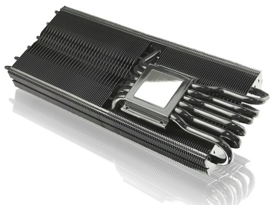
No you can't, but read on. When we 
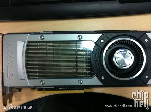
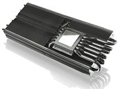
learned that NVIDIA's upcoming GeForce GTX 770 uses a GPU not unlike the GeForce GTX 680 in specifications, we overlooked one possibility, that it uses the same exact chip, the GK104. We assumed that NVIDIA could release a new ASIC codenamed "GK114" or "GK204," which features higher energy-efficiency, and GPU Boost 2.0.

A Reddit user 
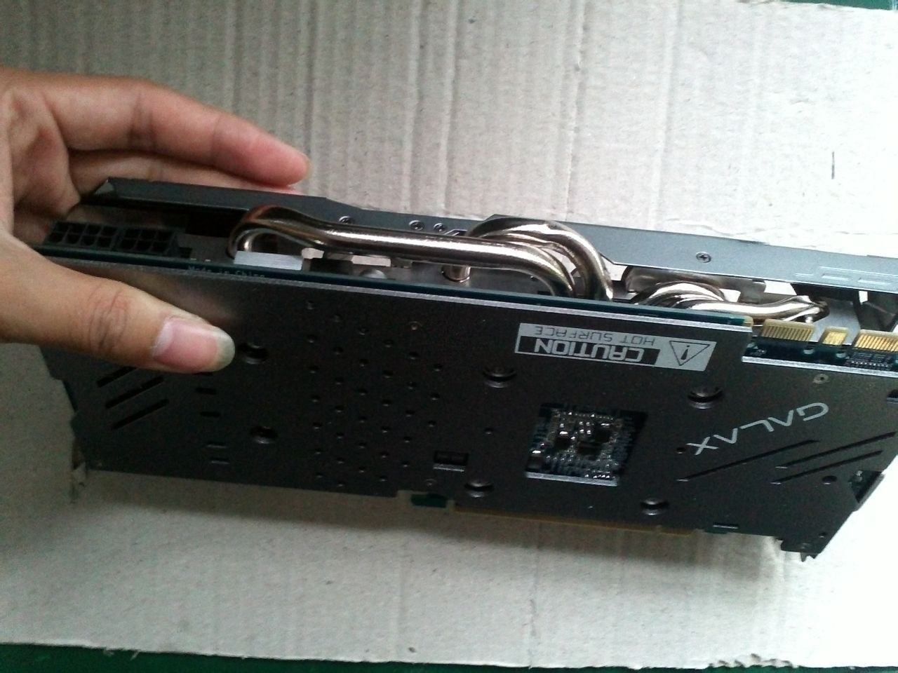
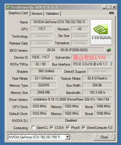
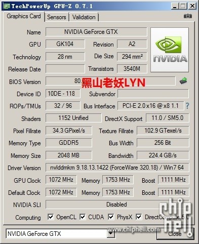
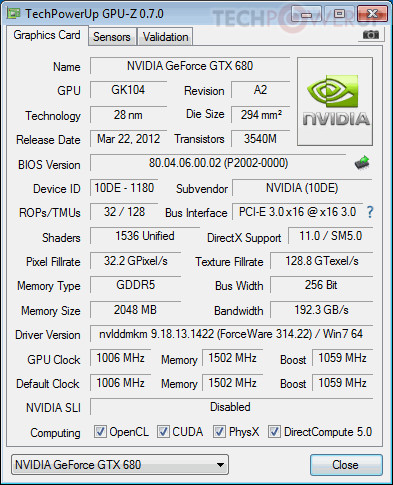
claims that a simple BIOS flash of the GeForce GTX 680 could turn it into a GeForce GTX 770. The BIOS ROM image, which probably works with reference-design GTX 680 boards was posted, along with a GPU-Z screenshot of a "GeForce GTX 770" obtained this way. The BIOS runs the card at 1059 MHz core, 1125 MHz maximum GPU Boost, and 1752 MHz (7.00 GHz GDDR5-effective) memory, yielding a memory bandwidth of 224 GB/s. The BIOS file can be found 
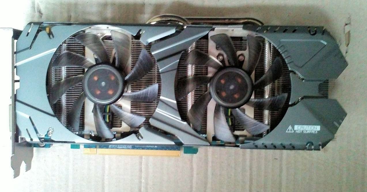
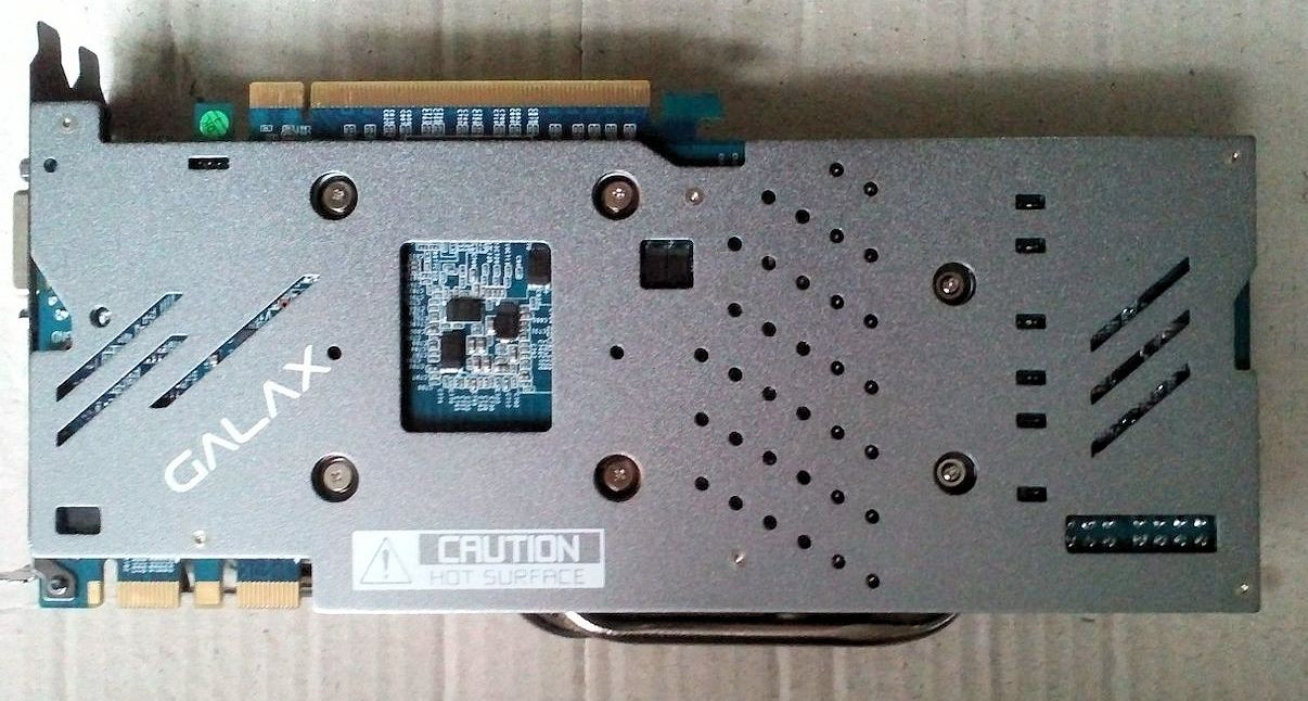
here (try it at your own risk). We tested the BIOS with some of our own GTX 680 cards, and found it to be nothing more than a modified GTX 680 BIOS (for increased clocks) with a modified driver INF file that makes the GeForce driver display a different model name. The BIOS just has made-up clock speeds that could run on some GTX 680 cards, but could be unstable on most.

We created four additional GPU-Z screenshots to serve as evidence that just by modifying the INF file, you can make the card appear as anything you want. The string from the INF file is used in Windows for display purposes only; the graphics driver does not use it for anything else; certainly not feature detection.

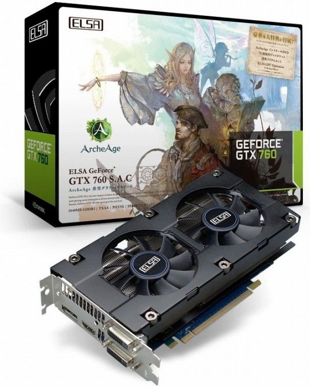
When your GTX 680 manages to be stable with the new BIOS, the higher clock speeds obviously work to get you that 5-7 percent performance increment. Third-rate companies often get away selling rebranded fake graphics cards in developing markets using this method. For example, they buy cheap GeForce 210 cards and sell them as GT 630 for twice the money. Even between officially rebranded NVIDIA graphics cards (such as GeForce 8800 GT to 9800 GT), the device ID is changed, so there's no reason why NVIDIA won't do the same with the GTX 770. In conclusion, this "GTX 770" mod is nothing more than a combination of a custom GTX 680 BIOS that adds higher clock speeds, and a custom INF file that changes the card's name string.

Are These GeForce GTX 780 and GeForce GTX 770?

NVIDIA's next-generation GPU family is not far away. We're hearing that new product-launches from the GPU giant could be just weeks away, and within this month. It's only natural that some of these cards could pass through leaky pipes, much to our benefit. One such source in China posted pictures of what he claims to be NVIDIA-reference design GeForce GTX 780 and GeForce GTX 770. Both cards feature a design not unlike the $1000 GeForce GTX TITAN. In fact they look identical. It's not the questionable embossing on the cooler shrouds that caught our attention, it's the subtle differences near the PCI-Express interface - location of PCB number, arrangement of termination resistors, etc., that did, and so we're rating this leak highly plausible.

We know from a previous report that GeForce GTX 780 will be positioned a notch below the GeForce GTX TITAN, in NVIDIA's product stack. It could be based on the same GK110 silicon, and could feature 2,496 CUDA cores, and a 320-bit wide GDDR5 memory interface, holding 5 GB of memory. It won't surprise us if NVIDIA completely recycles the GTX TITAN PCB, as it doesn't particularly have an over-the-top selection of components, apart from the GPU. The GeForce GTX 770 is a different beast altogether. It is based on a GPU not unlike the GK104, with 1,536 CUDA cores, and a 256-bit wide GDDR5 memory interface, holding 4 GB of memory. To sweeten the prospect of upgrading to these new cards, NVIDIA is dropping in the same sexy magnesium alloy-based cooling solution it used on $1000 cards such as the GTX TITAN and GTX 690.

Gigabyte Unveils GeForce GTX 660 Ti WindForce III 3 GB Graphics Card

Gigabyte unveiled a variation of its 3 GB GeForce GTX 660 Ti OC graphics card. Bearing the model number N66TWF3-3GD, the card sticks to NVIDIA reference clock speeds of 915/980/6008 MHz (core/GPU Boost/memory). It features WindForce 3 triple-fan cooler featuring three 80 mm fans, ventilating a complex heatpipe-fed heatsink. Based on the 28 nm GK104 GPU, the GeForce GTX 660 Ti packs 1344 CUDA cores, and a 192-bit wide GDDR5 memory interface. On this card, twelve 2 Gbit GDDR5 chips are used, arranged on either sides of the PCB. Expect the card to cost around 300€.

Colorful Unveils GeForce GTX 660 Ti World Cyber Games Edition Graphics Card

Colorful unveiled a limited edition GeForce GTX 660 Ti iGame graphics card that's hand-painted to celebrate World Cyber Games 2012 Final, which was recently held in Shanghai, China. Its cooler shroud features streaks and patterns of multiple colors. Why? Because it's Colorful, that's why! In addition to dual-fan cooler that looks more than capable to handle the 150W GPU, Colorful included detachable auxiliary heatsinks that are part of the "Air Kit."

The card features a 4+2 phase VRM that draws power from two 6-pin PCIe power connectors, redundant BIOS loaded in two separate EEPROM chips, and 2 GB of GDDR5 memory across a 192-bit wide memory interface. Based on the 28 nm GK104 silicon, the GeForce GTX 660 Ti packs 1344 CUDA cores. Colorful manufactured very small numbers of these cards, which will be sold in the Greater China region, some of the cards could make it to Europe.

NVIDIA Announces GeForce GTX 680MX, GTX 675MX and GTX 670MX Mobile GPUs

NVIDIA added three new high-performance mobile GPUs to its lineup, the GeForce GTX 680MX, GeForce GTX 675MX, and GeForce GTX 670MX. Based on the 28 nm GK104 silicon, the GTX 680MX topples GTX 680M as NVIDIA's (and perhaps, the world's) most powerful GPU for notebooks. While the GTX 680M features 1344 CUDA cores, with 720 MHz core and 3.60 GHz memory, the new GTX 680MX features 1536 CUDA cores, with the same 720 MHz clock speed, but faster 5.00 GHz memory. 2 GB of GDDR5 memory is standard issue for this chip.

Moving on, NVIDIA created a new SKU that takes position between the Fermi architecture-based GTX 675M, and the GTX 680M. Called the GTX 675MX, the new SKU is also based on the GK104 silicon, but configured with 960 CUDA cores, and 2 GB of GDDR5 memory across a 256-bit wide memory interface. The core is clocked at 600 MHz, and memory at 3.60 GHz. The last of the three is the new GTX 670MX, based on the 28 nm GK106 silicon. Like the GTX 675MX, it is configured with 960 CUDA cores (the full compliment of GK106), but with a narrower memory interface, that's 192-bit wide. Its core is clocked at 600 MHz, and memory at 2.80 GHz. 2 GB GDDR5 is the standard memory amount. Expect a wave of performance notebooks and all-in-one desktops to feature these new chips.

ZOTAC GeForce GTX 660 Ti Extreme Graphics Card Detailed

To the rest of the world, ZOTAC's fastest GeForce GTX 660 Ti offering is the AMP! Edition, but select markets in the Greater China region have access to the good stuff, the GTX 660 Ti Extreme. Built for competitive overclocking, the GTX 660 Ti Extreme from ZOTAC features in the same GamerForce series as the GTX 670 Extreme and GTX 680 Extreme. Except the change in color scheme of the cooler shroud (which is now black+gold), and the narrower memory bus interface, the card is virtually identical to the GTX 670 Extreme.

The GTX 660 Ti Extreme features the same exact PCB design as the one used on the GTX 670 and GTX 680 Extreme graphics cards. With the exception of two empty 32-bit wide memory pads, the PCB designs are identical. The PCB retains the 13-phase VRM that draws power from 6-pin and 8-pin power connectors, OC+ module support, and the beastly dual 92 mm fan-heatsink. The cooler uses five 8 mm-thick nickel-plated copper heat-pipes to convey heat to a dense aluminum fin array, which is then ventilated by the two fans.
Return to Keyword Browsing
May 8th, 2024 01:25 EDT change timezone

New Forum Posts

Popular Reviews

Controversial News Posts