News Posts matching #GlobalFoundries

Return to Keyword Browsing

GLOBALFOUNDRIES Announces New Chief Executive to Lead Next Phase of Growth

Building on the successful track record of its first five years in the semiconductor industry and its continued commitment to build out its global network of manufacturing facilities, GLOBALFOUNDRIES announced today, from its new offices in Silicon Valley, Sanjay Jha has been appointed as the company's new Chief Executive Officer. Jha has served as CEO of Motorola Mobility Inc. and as the COO of Qualcomm Inc.

Ajit Manocha, who served as an advisor to the company's shareholder prior to being appointed CEO of GLOBALFOUNDRIES in mid-2011, will return to that role and will work closely with Jha on his transition.

Micron Technology Appoints Rajan Rajgopal as Vice President of Quality

Micron Technology, Inc. (Nasdaq:MU), today announced that the company has named Rajan Rajgopal, vice president of Quality. Rajgopal will be responsible for overseeing all aspects of Micron's quality systems including manufacturing, customer program management and product ramps. He brings more than 25 years of experience to Micron and most recently served as the vice president of Global Quality and Customer Enablement for GLOBALFOUNDRIES in Singapore.

"Micron continues to evolve as a memory business driven by systems-level solutions, and quality plays a heightened role in serving our valued customers," said Micron President Mark Adams. "We are excited to have Rajan join our team and leverage his experience in serving our customers in an increasingly diversified set of application segments."

RockChip Builds SoCs on GlobalFoundries' 28 nm HKMG Process

GLOBALFOUNDRIES and Fuzhou Rockchip Electronics Co., Ltd. today announced that Rockchip's next-generation mobile processors are ramping to production on GLOBALFOUNDRIES' 28 nm High-K Metal Gate (HKMG) process technology. Based on a multi-core ARM Cortex-A9 design, the RK3188 and RK3168 chips are optimized for tomorrow's high-performance, low-cost tablets that require long-lasting battery life (see product specifications in annex).

The combination of Rockchip's design and GLOBALFOUNDRIES' 28 nm HKMG process technology resulted in a mainstream tablet System-on-Chip (SoC) capable of operating at up to 1.8 GHz performance, while still maintaining the power efficiency expected by mobile device users. The chips began sampling to OEMs in early 2013 and are now ramping to support a wide range of manufacturers.

GLOBALFOUNDRIES Accelerates Adoption of 20nm-LPM and 14nm-XM FinFET Processes

At next week's 50th Design Automation Conference (DAC) in Austin, Texas, GLOBALFOUNDRIES will unveil a comprehensive set of certified design flows to support its most advanced manufacturing processes. The flows, jointly developed with the leading EDA providers, offer robust support for implementing designs in the company's 20nm low power process and its leading-edge 14nm-XM FinFET process. Working closely with Cadence Design Systems, Mentor Graphics and Synopsys, GLOBALFOUNDRIES has developed the flows to address the most pressing design challenges, including support for analog/mixed signal (AMS) design, and advanced digital designs, both with demonstration of the impact of double patterning on the flow.

The GLOBALFOUNDRIES design flows work with its process design kits (PDKs) to provide real examples that demonstrate the entire flow. The user can download the design database, the PDK, detailed documentation and multi-vendor scripts to learn how to set up and use the GLOBALFOUNDRIES design flow. The flows use open source examples and provide the customer with working, executable and customizable flows.

Globalfoundries and Infineon Collaborate for 40 nm Embedded Flash Process

Infineon Technologies and GLOBALFOUNDRIES Inc. today announced a joint technology development and production agreement for 40 nanometer (nm) embedded flash (eFlash) process technology. The cooperation will focus on technology development based on Infineon's eFlash cell design and manufacturing of automotive and security microcontrollers (MCUs) with 40nm process structures. Production of the next generation 40nm eFlash MCUs will take place at different GLOBALFOUNDRIES sites, initially in Singapore with subsequent transfer to its site in Dresden, Germany.

"Next generation embedded Flash microcontrollers with 40nm process structures will further enhance our competitive strength in the automotive as well as chip card and security markets," says Arunjai Mittal, Member of the Management Board of Infineon Technologies. "We trust in GLOBALFOUNDRIES with their excellent manufacturing background and sites on different continents to fulfill Infineon's stringent quality, infrastructure security and business continuity requirements."

AMD Reports 2013 First Quarter Results

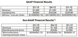
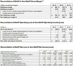
AMD (NYSE:AMD) today announced revenue for the first quarter of 2013 of $1.09 billion, an operating loss of $98 million and a net loss of $146 million, or $0.19 per share. The company reported a non-GAAP operating loss of $46 million and a non-GAAP net loss of $94 million, or $0.13 per share.

"Our first quarter results reflect our disciplined operational execution in a difficult market environment," said Rory Read, AMD president and CEO. "We have largely completed our restructuring and are now focused on delivering a powerful set of new products that will accelerate our business in 2013. We will continue to diversify our portfolio and attack high-growth markets like dense server, ultra low-power client, embedded and semi-custom solutions to create the foundation for sustainable financial returns."

Hybrid Memory Cube Consortium Finalizes Specifications

More than 100 developer and adopter members of the Hybrid Memory Cube Consortium (HMCC) today announced they've reached consensus for the global standard that will deliver a much-anticipated, disruptive memory computing solution. Developed in only 17 months, the final specification marks the turning point for designers in a wide range of segments-from networking and high-performance computing, to industrial and beyond-to begin designing Hybrid Memory Cube (HMC) technology into future products.

A major breakthrough with HMC is the long-awaited utilization of advanced technologies to combine highperformance logic with state-of-the-art DRAM. With this first HMC milestone reached so quickly, consortium members have elected to extend their collaborative effort to achieve agreement on the next generation of HMC interface standards.

GLOBALFOUNDRIES Demonstrates 3D TSV Capabilities on 20nm Technology

GLOBALFOUNDRIES today announced the accomplishment of a key milestone in its strategy to enable 3D stacking of chips for next-generation mobile and consumer applications. At its Fab 8 campus in Saratoga County, N.Y., the company has demonstrated its first functional 20nm silicon wafers with integrated Through-Silicon Vias (TSVs). Manufactured using GLOBALFOUNDRIES' leading-edge 20nm-LPM process technology, the TSV capabilities will allow customers to stack multiple chips on top of each other, providing another avenue for delivering the demanding performance, power, and bandwidth requirements of today's electronic devices.

TSVs are vertical vias etched in a silicon wafer that are filled with a conducting material, enabling communication between vertically stacked integrated circuits. The adoption of three-dimensional (3D) chip stacking is increasingly being viewed as an alternative to traditional technology node scaling at the transistor level. However, TSVs present a number of new challenges to semiconductor manufacturers.

GLOBALFOUNDRIES Offers Enhanced 55 nm CMOS Logic Process

GLOBALFOUNDRIES today announced additional enhancements to the foundry's 55-nanometer (nm) Low-Power Enhanced (LPe) process technology platform - 55nm LPe 1V - with qualified, next-generation memory and logic IP solutions from ARM. The 55nm LPe 1V is the industry's first and only enhanced process node to support ARM's 1.0/1.2V physical IP library, enabling chip designers to use a single process that supports two operating voltages in a single SoC.

"The key advantage of this 55nm LPe 1V offering is that the same design libraries can be used whether you are designing at 1.0 voltage or 1.2 voltage power option," said Bruce Kleinman, Vice President of Product Marketing at GLOBALFOUNDRIES. "What it means is that same set of design rules and models can be adopted, with no extra mask layer or special process required. This translates into cost saving and design flexibility without compromising on the power and optimization features."

Rambus Introduces R+ LPDDR3 Memory Architecture Solution

Rambus Inc., the innovative technology solutions company that brings invention to market, today announced its first LPDDR3 offering targeted at the mobile industry. In the Rambus R+ solution set, the R+ LPDDR3 memory architecture is fully compatible with industry standards while providing improved power and performance. This allows customers to differentiate their products in a cost-effective manner with improved time-to-market. Further helping improve design and development cycles, the R+ LPDDR3 is also available with Rambus' collaborative design and integration services.

The R+ LPDDR3 architecture includes both a controller and a DRAM interface and can reduce active memory system power by up to 25% and supports data rates of up to 3200 megabits per second (Mbps), which is double the performance of existing LPDDR3 technologies. These improvements to power efficiency and performance enable longer battery life and enhanced mobile device functionality for streaming HD video, gaming and data-intensive apps.

Nitero Demos 60 GHz Wi-Fi Solution on GLOBALFOUNDRIES' 65 nm-LPe RF Technology

Today at the 2013 Consumer Electronics Show (CES), Nitero, a fabless semiconductor company developing next-generation Wi-Fi solutions for mobile devices, demonstrated its innovative 60 GHz Wi-Fi solution manufactured on GLOBALFOUNDRIES' 65 nanometer (nm) Low Power Enhanced (LPe) RF platform optimized for mobile SoC applications.

Nitero's 60 GHz solution, which complements and completes today's Wi-Fi solutions such as 802.11n and 802.11ac, eliminates the need for physical connectors and their cables, dramatically increasing ease-of-use in tablet and handset devices. The company's multi-gigabit, ultra-low power Wi-Fi solution allows consumers to enjoy the same capabilities and flexibility of high-end notebook computers in the convenient portability of a mobile device. Compliant with the now IEEE ratified 802.11ad industry standard, Nitero plans for its upcoming solution to be Wi-Fi CERTIFIED for popular solutions from the Wi-Fi Alliance such as Wi-Fi Direct and Miracast.

GLOBALFOUNDRIES to Build R&D Facility in New York

GLOBALFOUNDRIES today announced plans to build a new global R&D facility at its Fab 8 campus in Saratoga County, N.Y. The new Technology Development Center (TDC) is expected to play a key role in the company's strategy to develop innovative semiconductor solutions allowing customers to compete at the leading edge of technology.

The TDC will feature more than a half million square feet of flexible space to support a range of technology development and manufacturing activities, including cleanroom and laboratory space. Representing an investment of nearly $2 billion, the facility will increase the total capital investment for the Fab 8 campus to more than $8 billion. Construction of the TDC is planned to begin in early 2013 with completion targeted for late 2014. Since breaking ground on Fab 8 in 2009, GLOBALFOUNDRIES has created approximately 2,000 new direct jobs and that number is expected to grow by another 1,000 employees for a total of about 3,000 new jobs by the end of 2014.

AMD Amends Wafer Supply Agreement With GLOBALFOUNDRIES

AMD today announced that it successfully amended its Wafer Supply Agreement (WSA) with GLOBALFOUNDRIES Inc.
The closure of amendment negotiations solidifies AMD's new operating model as communicated at the third quarter 2012 earnings announcement.

To better align with today's PC market dynamics, AMD and GLOBALFOUNDRIES agreed on purchase commitments for fourth quarter 2012 and established fixed pricing and other terms of the WSA which apply to products AMD will purchase from GLOBALFOUNDRIES through Dec. 31, 2013.

GLOBALFOUNDRIES, IBM, Intermolecular Collaborate to Speed Advanced Logic Development

Intermolecular, Inc. today announced that GLOBALFOUNDRIES and IBM will leverage Intermolecular's High Productivity Combinatorial (HPC) technology, as the companies work to speed development of manufacturing technologies down to the 10 nm node.

Intermolecular's combinatorial technology allows many more tests to be done using a single wafer. This enables experimental data to be generated and analyzed with significantly greater speed and efficiency than a traditional development line, accelerating innovation in materials, processes, and device architectures.

GLOBALFOUNDRIES Unveils FinFET Transistor Architecture for Next-Gen Mobile Devices

GLOBALFOUNDRIES today accelerated its leading-edge roadmap with the launch of a new technology designed for the expanding mobile market. The company's 14nm-XM offering will give customers the performance and power benefits of three-dimensional "FinFET" transistors with less risk and a faster time-to-market, helping the fabless ecosystem maintain its leadership in mobility while enabling a new generation of smart mobile devices.

The XM stands for "eXtreme Mobility," and it is the industry's leading non-planar architecture that is truly optimized for mobile system-on-chip (SoC) designs, providing a whole product solution from the transistor all the way up to the system level. The technology is expected to deliver a 40-60% improvement in battery life when compared to today's two-dimensional planar transistors at the 20 nm node.

GLOBALFOUNDRIES Appoints Joe Chen as New Sales Head for Greater China

GLOBALFOUNDRIES today announced that Joe Chen has been appointed as the new Vice President of Sales for the Greater China region, joining the company from Marvell Technology, a leading provider of storage, communications and consumer semiconductor products.

"Joe will play a key role in driving our sales strategy in the growing markets in Asia"
In this role, Chen will be responsible for sales in the Greater China region consisting of China and Taiwan. He will build and mentor a top-quality regional sales team, and grow and maintain successful and trusted partnerships with existing and new customers to expand the company's market share in Asia. Chen reports to Chuck Fox, Senior Vice President of Worldwide Sales at GLOBALFOUNDRIES.

GLOBALFOUNDRIES Adds New Vice President of Product Marketing

GLOBALFOUNDRIES today announced the addition of Bruce Kleinman as vice president of product marketing. Based at the company's corporate offices in Silicon Valley and reporting to Mike Noonen, executive vice president of worldwide marketing and sales, Kleinman will lead the GLOBALFOUNDRIES product marketing efforts, working with global customers to help develop and define product offerings and customer value propositions.

"GLOBALFOUNDRIES offers several unique value propositions anchored around technology, global capacity, service and flexibility, and our investment of resources globally to support the world's semiconductor and technology companies," said Mike Noonen, executive vice president, worldwide marketing and sales. "Bruce brings more than 25 years of sales, business development, marketing and engineering experience to GLOBALFOUNDRIES and we're excited to welcome him to our growing global team."

ARM and GLOBALFOUNDRIES Collaborate to Enable Devices on 20 nm and FinFET

GLOBALFOUNDRIES and ARM today announced a multi-year agreement to jointly deliver optimized system-on-chip (SoC) solutions for ARM processor designs on GLOBALFOUNDRIES' 20-nanometer (nm) and FinFET process technologies. The new agreement also extends the long-standing collaboration to include graphics processors, which are becoming an increasingly critical component in mobile devices. As part of the agreement, ARM will develop a full platform of ARM Artisan Physical IP, including standard cell libraries, memory compilers and POP IP solutions. The results will help enable a new level of system performance and power-efficiency for a range of mobile applications, from smartphones to tablets to ultra-thin notebooks.

The companies have been collaborating for several years to jointly optimize ARM Cortex-A series processors, including multiple demonstrations of performance and power-efficiency benefits on 28nm as well as a 20nm test-chip implementation currently running through GLOBALFOUNDRIES fab in Malta, N.Y. This agreement extends the prior efforts by driving production IP platforms that will enable customer designs on 20nm and promote rapid migration to three-dimensional FinFET transistor technology. This joint development will enable a faster time to delivering SoC solutions for customers using next-generation ARM CPUs and GPUs in mobile devices.

AMD Announces Pricing of Private Offering of $500 Million of Senior Notes

AMD today announced that it has agreed to sell $500 million aggregate principal amount of its 7.50% Senior Notes due 2022 in a private offering. AMD intends to close the transaction on or around August 15, 2012. AMD estimates that the net proceeds from the issuance and sale of the senior notes will be approximately $491 million after deducting the initial purchasers' discounts and estimated offering expenses.

AMD intends to use the net proceeds for general corporate purposes and working capital, which may include the following: (i) the repayment or repurchase of some or all of its outstanding 5.75% Convertible Senior Notes due 2012, (ii) repayment or repurchase of some or all of its outstanding 6.00% Convertible Senior Notes due 2015, (iii) cash payments to GLOBALFOUNDRIES related to the 28nm product limited waiver of exclusivity, or (iv) potential strategic transactions.

AMD Announces Private Offering of $300 Million of Senior Notes

Advanced Micro Devices, Inc. (NYSE: AMD) today announced that it intends to commence a private offering, subject to market and other conditions, of $300 million aggregate principal amount of senior notes due 2022. AMD intends to use the net proceeds for general corporate purposes and working capital, which may include the following: (i) the repayment or repurchase of some or all of its outstanding 5.75% Convertible Senior Notes due August 2012, (ii) repayment or repurchase of some or all of its outstanding 6.00% Convertible Senior Notes due 2015, (iii) cash payments to GLOBALFOUNDRIES related to the 28nm product limited waiver of exclusivity, or (iv) potential strategic transactions.

The new senior notes have not been registered under the Securities Act of 1933, as amended, or applicable state securities laws, and will be offered only to qualified institutional buyers in reliance on Rule 144A and in offshore transactions pursuant to Regulation S under the Securities Act of 1933, as amended. Unless so registered, the new senior notes may not be offered or sold in the United States except pursuant to an exemption from the registration requirements of the Securities Act and applicable state securities laws.

GLOBALFOUNDRIES Extending Fab 8 to Meet Strong Customer Demand

GLOBALFOUNDRIES today announced it is moving forward with the final construction for the extension of Module 1 at the Fab 8 campus in New York. The project will add 90,000 square feet of manufacturing capacity, bringing the total capacity for Fab 8 Module 1 to 300,000 square feet. Construction activities are scheduled to begin in August and work is expected to be completed in December 2013.

"During the construction of Fab 8, we extended the shell of the Module 1 building with the expectation that our business would continue to grow. Today we see increasingly strong demand from our customers, especially at the 28nm node, and we are excited to be moving forward with this next phase in the development of the Fab 8 campus," said Eric Choh, vice president and general manager, Fab 8, GLOBALFOUNDRIES. "By continuing to expand our investment in the project, GLOBALFOUNDRIES is delivering more options to our global customers, while helping to redefine upstate New York as a premier hub of the global semiconductor industry, creating thousands of new advanced manufacturing jobs, and contributing billions of dollars to the regional economy."

GLOBALFOUNDRIES Silicon Validates 28nm AMS Production Design

At next week's Design Automation Conference (DAC) in San Francisco, Calif., GLOBALFOUNDRIES plans to demonstrate an enhanced silicon-validated design flow for its 28nm Super Low Power (SLP) technology with Gate First High-k Metal Gate (HKMG). The flow provides proven and complete front-to-back support for advanced analog/mixed-signal (AMS) design using the industry's latest design automation technology. In addition, the company will reveal jointly developed design flows with its EDA partners in certifying both analog and digital "double patterning aware" flows for its 20nm process, with silicon validation expected in early 2013 at that technology node.

As a result of GLOBALFOUNDRIES' commitment to silicon validation of flows before releasing them, customers have the confidence to produce signoff-ready 28nm digital and analog designs using the industry's most advanced set of design tools, tool scripts, and methodologies from the leading EDA suppliers. The company's tight collaboration with the design tool and IP ecosystem also accelerates its ability to develop working flows for advanced nodes such as 20nm, providing their advantages in gate density, performance, and lower power to customers ahead of other foundries.

GLOBALFOUNDRIES Improves IC Reliability with Customized Circuit Checks

Mentor Graphics Corp. today announced that GLOBALFOUNDRIES is helping its customers improve reliability checking by adding Calibre PERC to select 28nm bulk CMOS design enablement flows. Calibre PERC will give designers access to the new reliability verification rules developed by the IBM Semiconductor Development Alliance (ISDA), augmented with GLOBALFOUNDRIES specific checks to help prevent external latch-up. Using Calibre PERC's unique architecture, complex reliability rules that require the integration of logical (net list) and layout (GDS) information can be fully automated, eliminating manual spreadsheet-based efforts and reducing the chances of design errors.

"In the past, verification of latch-up immunity depended on manual layout checks and rough approximations of device and interconnect resistance using traditional mechanisms," said Bill Liu, vice president of design enablement at GLOBALFOUNDRIES. "Now our customers can perform accurate measurements and analysis automatically using Calibre PERC's data integration capability. For example, some of our customers are currently using PERC to accurately determine the resistance of the paths in complex output driver arrays as a function of device spacing. This allows them to easily and accurately detect points in the circuit where latch-up could be an issue and to make appropriate improvements."

GLOBALFOUNDRIES Fab 8 Adds Tools to Enable 3D Chip Stacking at 20nm and Beyond

GLOBALFOUNDRIES today announced a significant milestone on the road to enabling 3D stacking of chips for next-generation mobile and consumer applications. At its Fab 8 campus in Saratoga County, NY, the company has begun installation of a special set of production tools to create Through-Silicon Vias (TSVs) in semiconductor wafers processed on the company's leading-edge 20nm technology platform. The TSV capabilities will allow customers to stack multiple chips on top of each other, providing another avenue for delivering the demanding requirements of tomorrow's electronic devices.

Essentially vertical holes etched in silicon and filled with copper, TSVs enable communication between vertically stacked integrated circuits. For example, the technology could allow circuit designers to place stacks of memory chips on top of an application processor, which can dramatically increase memory bandwidth and reduce power consumption-a key challenge for designers of the next generation of mobile devices such as smartphones and tablets.

Abu Dhabi and Saxony to Host Twin Semiconductor Research Labs

The Advanced Technology Investment Company and the state of Saxony, Germany, today announced the establishment of two research labs working in tandem on areas of interest to the semiconductor industry. The 'Twin Labs' project will be backed by the Advanced Technology Investment Company (ATIC) and Saxony, which have each pledged US$2.4 million towards the plan over two years. Masdar Institute of Science and Technology will host the Abu Dhabi research center, while Technische Universität Dresden will oversee development of the Saxony lab.

Both sites will be of similar size, initially staffed with 10-12 graduate/Ph.D. students. Additional faculty members will be engaged at a later stage after the centers have established initial successes. Research will focus primarily on three-dimensional chip stacking, a potentially faster and more energy efficient semiconductor technology that follows ATIC's broader emphasis on minimum electronic energy systems, or MEES.
Return to Keyword Browsing
Apr 3rd, 2025 05:36 EDT change timezone

New Forum Posts

Popular Reviews

Controversial News Posts