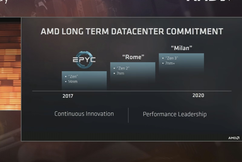
AMD Fast-tracks 7nm "Navi" GPU to Late-2018 Alongside "Zen 2" CPU
AMD is unique in the world of computing as the only company with both high-performance CPU and GPU products. For the past several years we have been executing our multi-generational leadership product and architectural roadmap. Just in the last 18 months, we successfully introduced and ramped our strongest set of products in more than a decade and our business has grown dramatically as we gained market share across the PC, gaming and datacenter markets.
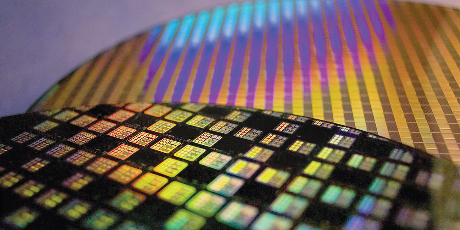
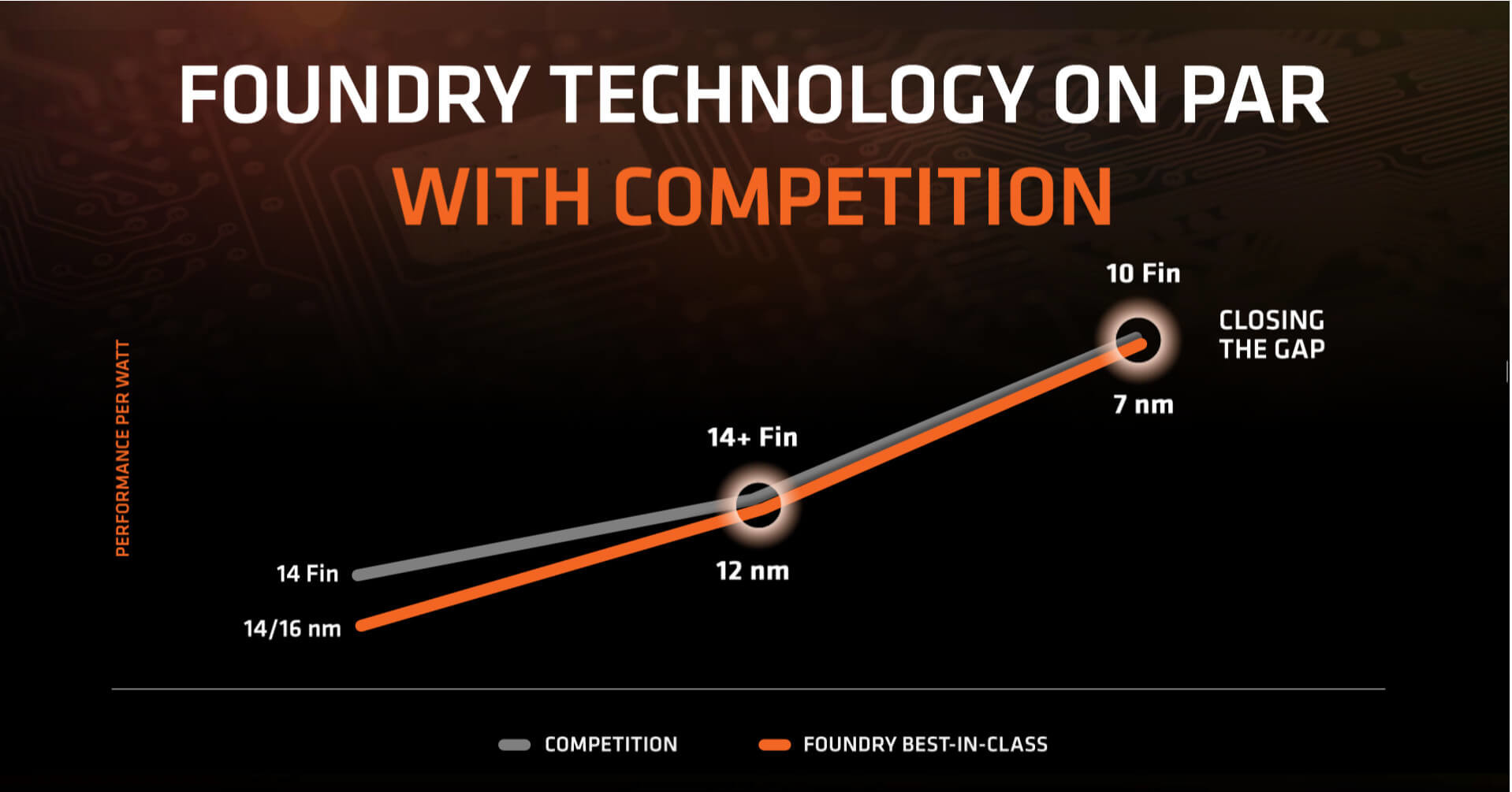
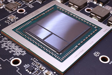
The industry is at a significant inflection point as the pace of Moore's Law slows while the demand for computing and graphics performance continues to grow. This trend is fueling significant shifts throughout the industry and creating new opportunities for companies that can successfully bring together architectural, packaging, system and software innovations with leading-edge process technologies. That is why at AMD we have invested heavily in our architecture and product roadmaps, while also making the strategic decision to bet big on the 7nm process node. While it is still too early to provide more details on the architectural and product advances we have in store with our next wave of products, it is the right time to provide more detail on the flexible foundry sourcing strategy we put in place several years ago.
The industry is at a significant inflection point as the pace of Moore's Law slows while the demand for computing and graphics performance continues to grow. This trend is fueling significant shifts throughout the industry and creating new opportunities for companies that can successfully bring together architectural, packaging, system and software innovations with leading-edge process technologies. That is why at AMD we have invested heavily in our architecture and product roadmaps, while also making the strategic decision to bet big on the 7nm process node. While it is still too early to provide more details on the architectural and product advances we have in store with our next wave of products, it is the right time to provide more detail on the flexible foundry sourcing strategy we put in place several years ago.