News Posts matching #Graphics CoreNext

Return to Keyword Browsing

AMD to Launch New GPUs and APUs Only After March: CEO

In its an investor conference-call following its Q4-2014 and FY-2014 results, AMD stated that it will release new GPU and APU products starting Q2-2015, or only after March. "Going into the second quarter and the second half of the year with our new product launches, I think we feel very good about where we are positioned there," said Lisa Su, chief executive officer.

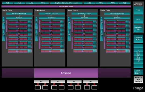
Q2-2015 will start off with the company's "Carrizo" line of all-in-one and notebook APUs. These chips will integrate the company's new "Excavator" CPU cores, with an integrated graphics core based on Graphics CoreNext 1.2 architecture (the same one AMD built its "Tonga" GPU on). Around the same time, AMD will launch new Opteron "Seattle" enterprise CPUs, which integrate up to eight ARM Cortex A-57 64-bit cores, targeting the ultra-dense server market. In Q2-2015, AMD will launch its latest Radeon Rx 300 series graphics processors. Its performance-segment part, the R9 380, will feature 4,096 GCN 1.2 cores, double that of its predecessor, and 4 GB of stacked HBM (high-bandwidth memory). Its mid-range chip, codenamed "Trinidad" will succeed "Curacao," and offer performance competitive to the $200-ish price-point.

AMD to Switch to GlobalFoundries' 28 nm SHP Node in 2015

Faced with continuous development roadblocks with TSMC, AMD is reportedly planning to switch to the 28 nm SHP process of GlobalFoundries, to build GPUs in 2015. The 28 nm SHP (super high-performance) node will allow the company to lower voltages, giving it greater room to increase clock speeds of its upcoming GPUs. AMD's GPUs in 2015 could be based on its latest Graphics CoreNext 1.2 architecture, and AMD needs every means to minimize voltages, and crank up clock speeds.

The company hasn't abandoned TSMC completely just yet, with reports speaking of AMD using the Taiwanese fab's 16 nm FinFet node to manufacture its next-generation "Zen" CPUs. Zen is the successor to AMD's "Bulldozer" architecture and its derivatives ("Piledriver" and "Steamroller.") It could feature a radically different core design.

AMD to Give 20 nm Optical Shrinks to Console SoCs First

AMD has the unique distinction of supplying SoCs to all three leading game console vendors simultaneously - Microsoft, Sony, and Nintendo. The company, like NVIDIA, is looking forward with perched eyes for manufacturing partner TSMC to get its 20 nanometer silicon fabrication node running full-cylinders. Unlike NVIDIA, which may use the new process to shrink its GPUs, or launch bigger chips based on its "Maxwell" architecture, AMD will treat its console SoCs with optical-shrinks to the new nodes first, so the company could immediately eke out better margins, as console gamers upgrade to Xbox One or the PlayStation 4.

AMD's SoC for the Xbox One, could be the first in line for this optical shrink to 20 nm. This chip features a transistor count of 5 billion, and houses eight 64-bit x86 CPU cores, and a 768 SP GPU based on the Graphics CoreNext architecture; 48 MB of on-die cache, and a quad-channel DDR3 IMC. The chip also features an integrated core logic. AMD's chip for the PlayStation 4 features design inputs from Sony. The chip features the same CPU component, but a 1152 SP GPU, and a 256-bit wide GDDR5 memory interface, wired to 8 GB of memory that's virtualized for both system- and graphics-memory. The 20 nm shrinks of both chips are expected to lower not just manufacturing costs, but also step up energy-efficiency, which could then let Microsoft and Sony save additional costs on other components, such as power and cooling.

AMD "Tonga" Silicon Features 384-bit Wide Memory Interface

In what could explain the rather large die-size and transistor-count of AMD's "Tonga" silicon, compared to "Tahiti," it turns out that the silicon features a 384-bit wide GDDR5 memory interface, and not the previously thought of 256-bit wide one. The die is placed on a package with pins for just 256-bit, on the Radeon R9 285, but it can be placed on a bigger package, with more pins, to wire out the full width of the memory bus, in future SKUs. This isn't the first time AMD has done something like this. Its "Tahiti LE" chip was essentially a "Tahiti" die placed on a smaller package with pins for just a 256-bit wide memory bus, on the oddball Radeon HD 7870 XT.

What this means is that AMD's next performance-segment graphics card based on the "Tonga" silicon, could feature 50% more memory bandwidth than the R9 285. The stream processor count is still 2,048, but these are more advanced Graphics CoreNext 1.2 stream processors, compared to first-generation ones on "Tahiti," offering more performance per Watt. The TMU count remains 128, although there's no clarity on the ROP count. Estimates are split between 32 and 48. The R9 285 has 32, and so does "Tahiti."

XFX Rolls Out its Radeon R9 285 Double Dissipation Graphics Card

XFX joined the Radeon R9 285 launch party with its compact R9 285 Double Dissipation graphics card. Built on an black, custom-design, matte-finish PCB, XFX' card features a lightweight version of its twin-fan cooling solution, which has been featured on its older performance-segment cards, such as the R9 270X. The cooler features a dense aluminium fin stack, to which heat is fed by four 6 mm thick copper heat pipes, which is then ventilated by a pair of 80 mm spinners. The card sticks to AMD reference clock speeds of 918 MHz core, and 5.50 GHz (GDDR5-effective) memory. Based on the 28 nm "Tonga" silicon, the R9 285 features 1,792 Graphics CoreNext 1.2 stream processors, 112 TMUs, 32 ROPs, and a 256-bit wide GDDR5 memory interface, holding 2 GB of memory on this card. Expect it to be priced at US $249.

AMD Announces the Radeon R9 285 Performance Graphics Processor

AMD announced its most important GPU for the season, the Radeon R9 285. The chip is designed to compete with the GeForce GTX 760 from NVIDIA at not just performance, but also energy-efficiency, and low component costs, so AMD can price it better. Based on a brand new 28 nm silicon by the company, codenamed "Tonga," the R9 285 features 1,792 Graphics CoreNext 1.2 stream processors, 112 TMUs, 32 ROPs, and a 256-bit wide GDDR5 memory interface, holding 2 GB of memory.

AMD partners are free to come up with 4 GB variants. The card supports DirectX 12, OpenGL 4.4, and Mantle. It features new AMD innovations, such as XDMA CrossFire, TrueAudio DSP, and 4-display Eyefinity by plugging into every connector on the card (two dual-link DVI, one DisplayPort 1.2, and one HDMI 1.4a). The card draws power from a pair of 6-pin PCIe power connectors. Available now, the Radeon R9 285, from various AMD partners starts at US $249.

PowerColor Radeon R9 285 TurboDuo Detailed

Here are some of the first high-resolution pictures of the Radeon R9 285 TurboDuo graphics card by PowerColor. The card features a meaty custom-design cooling solution, with two twin-impeller fans, and a dense aluminium fin-stack heatsink. PowerColor didn't bother with a reference-clock variant of this card. It comes factory-overclocked, at 945 MHz core (918 MHz reference), and 5.50 GHz (GDDR5-effective) memory. It features 2 GB of it.

Based on the 28 nm "Tonga" silicon, the Radeon R9 285 features 1,792 Graphics CoreNext 1.1 stream processors, 112 TMUs, 32 ROPs, and a 256-bit wide GDDR5 memory interface. The card draws power from two 6-pin PCIe power connectors. Display outputs include two dual-link DVI, and one each of HDMI and DisplayPort. With a modern XDMA CrossFire interface, the card lacks CrossFire fingers. It remains to be seen just how many cards the driver allows you to run in tandem. The Radeon R9 285 from AMD will launch on the 2nd of September, 2014. Prices start at US $249.

ASUS Radeon R9 285 Strix Graphics Card Pictured

Here are some of the first detailed shots of ASUS' premium custom-design Radeon R9 285 Strix graphics card, based on AMD's upcoming GPU. The card features a unique cooling solution that keeps its fans off until the GPU reaches a temperature threshold. The cooler's underlying heatsink is essentially DirectCU II, featuring a dense aluminium fin stack to which heat drawn directly from the GPU die is fed by a number of nickel-plated copper heat pipes. This particular card features a factory-overclock, and 2 GB of memory. Oh, and it comes with a back-plate. Based on the 28 nm "Tonga" silicon, the R9 285 features 1,792 Graphics CoreNext 1.1 stream processors, 112 TMUs, 32 ROPs, and a 256-bit wide GDDR5 memory interface. The card is set to launch on 2nd September, 2014. It will start at US $249.

AMD Radeon R9 285 Clock Speeds and Pricing Revealed

It's confirmed the GeForce GTX 760 really is on AMD's crosshair's with the Radeon R9 285. Based on the 28 nm "Tonga" silicon, which is designed to offer "Tahiti" like performance at the energy-efficiency levels comparable to NVIDIA's GK104, the R9 285 features 1,792 Graphics CoreNext stream processors, 112 TMUs, 32 ROPs, and 256-bit wide GDDR5 memory interface, holding 2 GB or 4 GB of memory. The card will feature clock speeds of 918 MHz core, 5.50 GHz memory. AMD claims the R9 285 will be up to 15 percent faster than the GeForce GTX 760. It will start at US $249, with partners coming out with custom-designs on day-one (September 2nd, 2014).

All AMD Graphics CoreNext GPUs to Support DirectX 12: Company

AMD production manager Devon Nekechuk, speaking at the company's 30 Years of Graphics event, disclosed that all AMD GPUs based on the Graphics CoreNext architecture will support DirectX 12, Microsoft's next generation multimedia API. The company is already up-to-date on the DirectX feature-level support, with support for DirectX 11.2. The company isn't drumming that up too loud, probably because it's developing an ecosystem for its own/competing AMD Mantle 3D API.

AMD Radeon R9 285 Launch Date Revealed

AMD is set to launch its new performance-segment graphics card, the Radeon R9 285, on the 2nd September, 2014. Ahead of its launch, the company is expected to tease the card at its August 23rd press-event, celebrating 30 years of graphics and gaming. On that day, AMD will share "partial" details of the card.

The R9 285 is based on AMD's swanky new 28 nm "Tonga" silicon, which is being drummed up to be AMD's best answer to NVIDIA's GK104. The chip offers performance rivaling "Tahiti," at the power consumption of GK104. The R9 285 is being designed to offer performance roughly that of the Radeon R9 280, at energy-efficiency, and pricing to drop lead on NVIDIA's GeForce GTX 760. A month later, presumably in early October, the company plans to launch the faster R9 285X, offering performance comparable (if not higher than) the R9 280X, at the energy-efficiency levels of GTX 770. "Tonga" physically features 2,048 Graphics CoreNext 1.1 stream processors, 128 TMUs, 32 ROPs, and a 256-bit wide GDDR5 memory interface, which will hold 2 GB or 4 GB of memory.

AMD "Tonga" Silicon Features 2048 Stream Processors

According to a block diagram of AMD's new 28 nm "Tonga" silicon, it features the same amount of shading power as "Tahiti," if not more. The chip features a total of 2,048 Graphics CoreNext 1.1 stream processors, spread across 32 compute units (CUs). The chip also features 128 TMUs. The block diagram was part of press-material AMD distributed with its recently launched FirePro W7100 professional graphics card, which is based on "Tonga."

The W7100 uses just 28 of the 32 CUs, and hence features 1,792 stream processors. Other features of "Tonga," according to the block diagram, include a 256-bit wide GDDR5 memory interface, 32 ROPs, TrueAudio DSP, and a modern XDMA CrossFire interface. The first consumer graphics card based on this chip is the Radeon R9 285. It is expected to feature 1,792 stream processors, and offer performance rivaling the Radeon HD 7950 Boost at lower power draw, and priced to compete with the GeForce GTX 760. That could leave the possibility of a future "R9 285X" with the chip's full complement of stream processors.

AMD Readies 28 nm "Tonga" to Take on GM107

NVIDIA's energy-efficiency leap achieved on existing 28 nanometer process, using the "Maxwell" based GM107, appears to have rattled AMD. The company is reportedly attempting a super-efficient, 28 nm, mid-range chip of its own, codenamed "Tonga." The chip could power graphics cards that compete with the GeForce GTX 750 Ti and GTX 750. The chip is likely to be based on Graphics CoreNext 2.0 micro-architecture, the same one that drives "Hawaii," which means AMD isn't counting on the micro-architecture for efficiency gains. It could feature an evolution of PowerTune, which works closer to the metal than its existing implementation on "Hawaii." Other features could include Mantle, TrueAudio, and perhaps even XDMA CrossFire (no cables needed). The chip could be wired to up to 2 GB of memory.

Another equally plausible theory doing rounds is that "Tonga" could be a replacement to "Tahiti Pro," designed to compete with the GK104 at much lower power footprint (than "Tahiti"), so AMD could more effectively compete with the GeForce GTX 760. The chip could be similar in feature-set to "Tahiti," with a narrower memory bus (256-bit wide), but higher clock speeds to make up for it. If this theory holds true, then "Tonga" could disrupt both Tahiti Pro and "Curacao XT." Curacao XT (R9 270X) is designed to offer a value-conscious alternative to the $250 GTX 760. The R9 280 is competitive in performance, but takes a beating on the energy-efficiency front, and is also costlier to manufacture, due to the higher transistor count and four additional memory chips. We could hear more at Computex 2014.

AMD Radeon R9 Series Prices Cool Down

AMD stabilized end-user pricing of its Radeon R9 series graphics cards, restoring them to their original launch prices in most cases, and even lower in some. Pricing of most AMD Graphics CoreNext architecture-based GPUs inflated over the past 6 months, due to the frenzy created by Cryptocoin currency miners, who leveraged the chips' GPGPU performance to 'mine' currencies such as Litecoin. Sensing that high prices are driving gamers away from Radeon, AMD swung into action by dealing with the problem at two levels. First, VP Global Channel Sales, Roy Taylor micro-managed the supply chain in China, and next, the company dealt with distributors and retailers.

At the time of preparing this article, most Radeon R9 series-based graphics cards, including high-end ones such as the R9 290X, and non-reference cards, are back to their original price-points on US retailer Newegg.com. The R9 290X can now be had for as low as US $519.99 (launch-price $549.99, was inflated to $750), the R9 290 for $379.99 (launched at $399.99, was inflated to $600), the R9 280X as low as $279.99 (launched at $299.99, was inflated to $400); the R9 280 as low as $229.99 (launched at $249.99, was inflated to $280); and the R9 270X at $199.99 (was inflated as high as $250).

Microsoft to Talk DirectX 12 at GDC

Microsoft will present its first paper on DirectX 12, its next-generation multimedia API, at the Game Developers Conference (GDC), on the 20th of March, 2013. The event could include presentations by NVIDIA, AMD, Intel, and Qualcomm. It's not clear at this point if Microsoft will release developer tools and resources on that day, or simply outline the API to spur interest. If anything, it should gently nudge today's GPU manufacturers to make their future GPU designs ready for the API. There are currently no GPU families that we know of, which support DirectX 12. AMD's current Graphics CoreNext 2.0 GPUs, such as the Radeon R9 290X, support DirectX 11.2, while NVIDIA's "Maxwell" GPUs, such as the GeForce GTX 750 Ti, feature an identical API feature-level support to their "Kepler" predecessors.

AMD "Kabini" Low Power APU Lineup Detailed Some More

AMD's upcoming low-power APU lineup, based on a common silicon code-named "Kabini," will launch with no less than five models. These could include chips built in both the socketed AM1 FCPGA and BGA packages, to cater to different target form-factors. The series starts off at the bottom with the dual-core E1-2100 and E1-2150. The two feature CPU clock speeds of 1.00 and 1.05 GHz, respectively, 1 MB of L2 cache, and Radeon HD 8210 graphics. The HD 8210 features 128 stream processors based on the Graphics CoreNext architecture. The CPU cores, on the other hand, are based on the "Jaguar" micro-architecture.

Moving on, there's the E2-3800. It tucks in a quad-core CPU clocked at 1.30 GHz, 2 MB of L2 cache, and Radeon HD 8280 graphics. The features the same stream processor count of 128 as the HD 8210, but higher clock speeds. Going beyond the E-Series, we enter AMD's more popularized A-Series, with the A4-5000, A4-5050, and the A6-5200. The three are built in the AM1 package, and are not compatible with platforms that drive the bigger A-Series "Kaveri" chips. The A4-5000 and A4-5500 feature CPU clock speeds of 1.50 GHz and 1.55 GHz, respectively, and Radeon HD 8330 graphics, featuring 128 stream processors, but 500 MHz GPU clock - the highest in its class. The list also points to an A6-5200. We're not sure which silicon it's based on, but it's outfitted with a quad-core CPU clocked at 2.00 GHz, and Radeon HD 8400 graphics.

AMD Mantle Driver to Only Benefit Four GPUs Initially

Crushed your F5 key on AMD driver download page yet? Unless you have four very specific AMD Radeon GPUs, you can stop it right now. According to DICE, developers of the first game to take advantage of Mantle, the 3D graphics API AMD is introducing with its Catalyst 14.1 beta driver, will give tangible benefits to only four specific GPUs - Radeon R9 290X, R9 290 (non-X), R7 260X, and A-Series "Kaveri" APU-integrated R7 200 series.

Owners of all other Radeon GPUs, including those based on the Graphics CoreNext (GCN) architecture, such as the recently launched R9 280X and R9 270X, are out of luck, for now. AMD is still ironing out issues with Mantle on those other GCN GPUs. Interestingly, in the same press note, DICE posted performance numbers yielded on an HD 7970, which look promising. AMD is expected to release its Catalyst 14.1 beta driver a little later this week, as it's jousting with some last-minute bug-finds.

AMD A10-7700K "Kaveri" De-lidded

Here are the first pictures of an AMD A10-7700K "Kaveri" APU with its integrated heat-spreader (IHS, or 'lid') removed. Put next to its predecessors, "Richland," "Trinity," and "Llano," AMD's new APU silicon is its biggest for the DIY PC market, more so because it's built on the 28 nm silicon fab process, compared to its predecessors being built on 32 nm. The die measures roughly 245 mm², and packs a staggering 2.41 billion transistors.

Under the IHS, AMD is using a thermal paste to transport heat from the die, and not a solder. The chip should be easy to de-lid, if you know what you're doing. Kaveri integrates two "Steamroller" x86-64 CPU modules with two cores each, a total of 4 MB of L2 cache, a massive on-die GPU with 512 stream processors based on the Graphics CoreNext micro-architecture, a dual-channel DDR3 IMC with hUMA and DDR3-2400 native support; and a PCI-Express 3.0 root complex.

AMD Announces 4th Generation A-Series "Kaveri" Desktop APUs

AMD announced its 2014 A-Series APU for the desktop platform, code-named "Kaveri," after the southern-Indian river. Built in the new FM2+ package, the APUs run only on socket FM2+ motherboards based on the AMD A88X, A78, and A55 chipsets; while the socket itself can seat older FM2 APU families, "Trinity" and "Richland." In many ways, the socket transition is similar to that of socket AM3+. "Kaveri" sees AMD integrate two of its newest CPU and GPU micro-architectures, "Steamroller" for CPU, and Graphics CoreNext 2.0 for the GPU. "Kaveri" is also built on newer generation 28 nm silicon fab process.

"Steamroller" is an evolution of the same modular CPU core design as its predecessors, "Piledriver" and "Bulldozer." AMD promises a 10 percent improvement in performance clock-by-clock, per core, which falls in line with AMD's normal scheme of annual incremental performance updates on its CPU micro-architectures. A "Steamroller" module is a combination of two 64-bit x86 cores, which feature dedicated and shared components. "Kaveri" has two such modules, and so physically, it features a quad-core CPU.

AMD Catalyst 14.1 Beta to Include Mantle and TrueAudio Runtimes

At its CES press-meet, AMD detailed the upcoming versions of Catalyst Software Suite, which will be unified to include graphics and system drivers for both discrete AMD Radeon GPUs, and integrated AMD A-Series APUs; and AMD core-logic (chipsets). The biggest takeaway from the presentation, by AMD's Terry "CatalystMaker" Makedon, is that the company will release the first Mantle and TrueAudio runtime environments with the upcoming Catalyst 14.1 Beta, due for later this month. Mantle is AMD's ambitious attempt at a 3D graphics API to rival Direct3D and OpenGL, that's optimized for its Graphics CoreNext micro-architecture; while TrueAudio is a positional audio DSP that promises to make games and movies sound more realistic.

Mantle promises "great" performance improvements in Battlefield 4, the only AAA game that we know of, to make use of the API. Mantle support was expected to be added to the game as an update around this time, but DICE' plans fell off the track with publisher EA coming down hard on the studio for shipping a game that's riddled with bugs. DICE will most likely have to fix most of its bugs for the retail DirectX 11.1 game, before EA allows it to toy with updates that add support for new and experimental APIs, let alone expansion packs. In related news, Catalyst 14.1 Beta will introduce additions to its frame-pacing fix, that will soon support Ultra HD displays, and Eyefinity setups on non-XDMA (pre R9 290 series) GPUs.

Why the Litecoin Craze Hurts More Than Helps Brand AMD Radeon

Price wars between GPU makers are something to look forward to each year, as that's typically when you get the best bang for your buck. Such an optimal time to buy new graphics cards usually comes when both AMD and NVIDIA have launched a new graphics card lineup, each. AMD tends to launch its lineup first, followed by NVIDIA, which then begins a cycle of proactive and reactive price-cuts between the two, which churns up the $300 price-performance sweet-spot so well, that a purchase from that segment usually sets your PC up for the following three years. 2013-14 saw a major disruption to this cycle, Litecoin mining. Litecoin miners will hurt more than help brand AMD Radeon, here's why.

AMD to Roll Out Eyefinity Frame-Pacing Fix in January

AMD is reportedly releasing a fix for frame-pacing issues for Radeon-based systems with Eyefinity setups in January, 2014, according to an AnandTech report. This September, AMD rolled out the first fix into the frame-pacing issues that affected Radeon GPUs based on the Graphics CoreNext architecture, in which raw-framerate didn't come with the right pacing between each frame, resulting in display output that isn't fluid, which even caused accusations to fly from some quarters about how honest AMD really is with performance numbers of its GPUs.

The Catalyst update that rolled out in September 2013 resolved the problem for a majority of users - with single displays connected to single GPUs, but left out cases in which people use Eyefinity (single display head spanning across multiple physical displays), on CrossFireX (multi-GPU) setups. It was originally expected that AMD would release the so-called "phase 2" Catalyst driver update looking into frame-pacing issues this November, but since the month has passed, AMD has obviously hit a delay. AnandTech reports that delay could last as long as two months, and one should expect "phase 2" to come out only towards the later half of January, since in the first half, AMD, along with the rest of the industry, will be busy with the 2014 International CES, where it will launch its next-generation A-Series APUs, codenamed "Kaveri."

Gigabyte Rolls Out Radeon R7 250 OC with Large Air Cooler

Gigabyte rolled out a revision of its Radeon R7 250 OC graphics card, featuring its 100 mm fan-heatsink that featured on its Radeon R7 240 OC graphics card. The card features a blue Ultra Durable 2 PCB, with Gigabyte's in-house fan-heatsink design that uses a chunky aluminium block with copper core and spirally-projecting ridges, and a 100 mm fan ventilating it, suspended on a black ABS shroud. The card features a small factory-overclock on the GPU, at 1100 MHz, compared to AMD reference speeds of 1050 MHz. The 2 GB of DDR3 memory is left untouched at 1.80 GHz. Display outputs include dual-link DVI, D-Sub, and HDMI 1.4a. The card relies entirely on the PCI-Express bus for power. Based on the 28 nm "Oland" silicon, the Radeon R7 250 features 384 Graphics CoreNext stream processors, 24 TMUs, 8 ROPs, and a 128-bit wide memory interface. Expect this card to retail for $90.

AMD Announces the Radeon R9 290

AMD announced the Radeon R9 290, its second graphics card based on the swanky new "Hawaii" silicon. The card is a slight cut-down of the R9 290X, and features 2,560 Graphics CoreNext stream processors, 160 TMUs, 64 ROPs, and a 512-bit wide GDDR5 memory interface, holding 4 GB of memory. The core is clocked at 948 MHz, and the memory at 5.00 GHz, churning out a memory bandwidth of 320 GB/s. The reference design board of the R9 290 is practically identical to its older sibling. AMD is pricing the card at an impressive $399, a price at which it will make both the $330 GeForce GTX 770 and the $499 GeForce GTX 780 look repulsively overpriced. Non-reference boards are expected to arrive by late-November, in time for last-minute X'mas purchases.

$450 Pricing Looking Increasingly Likely for Radeon R9 290

MSRP (before taxes) pricing of AMD's upcoming Radeon R9 290 (non-X) being around $450 is looking increasingly likely. In a string of reports that Japanese publication Hermitage Akihabara published ahead of launches of the R9 290X and the R9 290, in which the publication talked about pricing in the country, a price difference of roughly 18 percent is emerging between the two. Applying that to the $549.99 MSRP of the R9 290X stateside, one can derive a $450 pricing for the R9 290. Granted, local taxation may greatly vary between Japan and other markets, affecting the end-user price, but pre-tax MSRPs can be consistent.

The Radeon R9 290 is expected to launch on the 5th of November, 2013. Based on the same "Hawaii" silicon as the Radeon R9 290X, it features 2,560 Graphics CoreNext stream processors, 160 TMUs, 64 ROPs, and a 512-bit wide GDDR5 memory interface, holding 4 GB of memory. Its core is clocked around 948 MHz, and memory at 5.00 GHz.
Return to Keyword Browsing
May 30th, 2024 08:51 EDT change timezone

New Forum Posts

Popular Reviews

Controversial News Posts