News Posts matching #Haswell

Return to Keyword Browsing

Ultrabooks to Grow Over 30% in 2013, Becoming Key PC Market Indicator

According to DRAMeXchange, a research division of TrendForce, as the cost decline of ultrabook components like SSDs, displays, and cases becomes more apparent next year and Intel places more focus on developing processors for ultrabook use, ultrabook market size may exceed 30 million units in 2013, growing by more than 30% compared to this year and accounting for 17% of the notebook market.

Intel to Begin Core "Haswell" Production in Q4

Despite a modest outlook for the PC industry looking into 2013, Intel plans to begin production of its 4th generation Core processors, codenamed "Haswell," on schedule, in Q4-2012. In the run up to Q4, Intel has taken stepped down production to prevent swelling of inventories. A little earlier this week, the company declared good Q3 results, turning $13.5 billion in gross revenue, and $3 billion in net income. In its press-release, CEO Paul Otellini acknowledged a increasingly tough environment was taking shape for the industry. "Our third-quarter results reflected a continuing tough economic environment," he said.

Intel: Low-Power Processors to Fuel Future of Mobile Computing Innovation

Intel Corporation's chief product officer today described how its low-power processors, starting with the company's 4th generation Intel Core processor family available next year, will set a new standard for mobile computing experiences and innovative Ultrabook, convertible and tablet designs.

Speaking at the Intel Developer Forum in San Francisco, David (Dadi) Perlmutter said Intel reduced the platform idle power of its 4th generation Intel Core processor family based on the next-generation "Haswell" microarchitecture by more than 20 times over the 2nd generation while delivering outstanding performance and responsiveness. He also said Intel will add a new line of even lower-power processors based on the same microarchitecture to its roadmap starting in 2013.

Despite Estimates Cuts, Analyst Bets on Haswell Success

Following last Friday's Q3 outlook lowering by Intel, market punters such as Merrill Lynch cut estimates. Vivek Arya, an analyst with the firm, cut its Q3 and Q4 estimates for Intel, while remaining optimistic about upcoming processes in the company's pitched battle with ARM in the lightweight SoC segment. Arya believes that with upcoming technologies, Intel has a fighting chance against ARM heavyweights. Said Arya in his report:
Next-gen chip manufacturing has become a 3-horse race between Intel, TSMC and Samsung, with Intel holding a 1 to 4 year lead, in our view. As we saw in 1H12, foundries were unable to ramp 28nm capacity, leading to product delays. Rising costs/ complexity (tri-gate) could further widen this gap. We believe this could enable Intel to gain a foothold (vs. zero today) in mobile over the next 2 years, as smartphone/tablet vendors look to Intel as a second or even primary source […] We firmly believe in Intel's ability to reliably produce the lowest cost and highest performance silicon can help it maintain a dominant position in servers/data centers (20% of sales, 10-15% CAGR), and transition from legacy PCs to next-gen smartphones, tablets, Ultrabooks and other converged devices in the next 1-2 years. Investors, meanwhile, benefit from a 3.6% div yield, $7.5bn in available buybacks (6% of mkt cap) and <10x PE.

Intel Ivy Bridge-E Slated for Q3-2013

Intel's next high-end desktop (HEDT) platform, codenamed "Ivy Bridge-E," is slated for Q3-2013, according to the latest platform road-map slide sourced by VR-Zone. According to the leaked slide, launch of Ivy Bridge-E Core i7 processors follows that of Core "Haswell" socket LGA1150 processors (Q2-2013). What's more, the upcoming Ivy Bridge-E chips will be compatible with existing socket LGA2011 motherboards, based on Intel X79 Express chipset.

Intel's next-generation Ivy Bridge-E chips are up-scaled versions of today's Core "Ivy Bridge" chips, built on the same 22 nm process, with more processing cores, memory channels, cache, and PCI-Express 3.0 certified system interfaces. It remains to be seen if Intel launches a new chipset to go with the new processor, or retains the X79 chipset with a few minor updates in the form of steppings. The company retained its X58 Express chipset over the first two HEDT processor generations (45 nm Core i7 "Bloomfield" and 32 nm Core i7 "Westmere").

Intel 8-series "Lynx Point" Chipset Models Surface

With its 22 nm "Ivy Bridge" CPU and 7-series "Panther Point" platform turning into a reality, Intel is moving on to development of the new 22 nm "Haswell" architecture. Entry-thru-performance segment Core "Haswell" processors will be built on the new LGA1150 package, and will be driven by a new series of platform controller hubs, codenamed "Lynx Point". We already know a tiny bit about the way Haswell+Lynx Point platform is structured, and the features that could come standard with it. A new VR-Zone report lists out all the chipset models Intel will carve out using the silicon.

The lineup is quite predictable. At the top of the pile is the feature-rich Z87, which has all the features of the platform, plus overclocking features. This is followed by Z85, which apart from features such as Rapid Storage Technology, could lack RAID for its SATA ports (could only feature AHCI and IDE modes). Then there's H87, which has all the features of Z87, except platform overclocking features. Q87 and Q85 are for large business desktops, and feature various client management features. Then there's B85, for small businesses. Lynx Point could feature as many as six SATA 6 Gb/s ports. Rapid Storage Technology will be updated to present users with a level of customization. Then there's Fast Boot, which speeds up system startup, provided an Intel SSD is used for caching.

Intel Haswell-EX Enterprise Processors To Introduce DDR4 Memory

The computing industry will see its next transition to a new memory standard only by 2014, and enterprise processors based on the "Haswell" microarchitecture will drive the change, according to a VR-Zone report. While client processors based on the Haswell architecture will retain current DDR3 memory standard with a possibility of higher DDR3 clock speeds, enterprise processors under the "Haswell-EX" family will feature the industry's first DDR4 memory controllers for x86. Following that, DDR4 will filter down to future client platforms. Pictured below, is a DDR4 UDIMM by Samsung.

FinalWire AIDA64 v2.30 Released

FinalWire today released the latest version of AIDA64, version 2.30. This release is set around enhancing the desktop gadget, improving the UPS and smart-battery monitoring capabilities, and adding support for newly-released hardware, such as the latest GPUs from AMD and NVIDIA; and the latest Intel SSDs. AIDA64 is proprietary software, and is available through FinalWire's online store.

DOWNLOAD: FinalWire AIDA64 2.30 EXE (installer), ZIP Package

The condensed change-log follows.

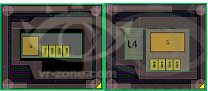
Haswell to Use 4th-Level On-Package Cache to Boost Graphics Performance

Intel is making serious efforts to boost CPU-integrated graphics performance using homegrown architectures, without having to borrow/license any technologies from the other two major players in the PC graphics business that have technological edges over Intel, and hence make high-performance discrete-GPUs (NVIDIA and AMD). Intel's architecture that succeeds Ivy Bridge, codenamed Haswell, will be at the receiving-end of a significant advancement in GPU performance.

We know from history, that Intel carves out variants of chips using a common silicon, by toggling the amount of L3 cache available, number of cores, and even number of iGPU shaders, apart from other natural handles such as clock speeds, voltages, and feature-set. With Haswell, the highest iGPU configuration will make use of a 4th-level cache (L4 cache), that sits on the package, while not being a part of the Haswell silicon. The Haswell silicon will instead be placed on a multi-chip module (MCM) along with a separate die that holds this L4 cache. The L4 cache will serve as a fast memory for the iGPU, while reducing or completely offloading the iGPU's dependency on the system memory as a frame-buffer (UMA).

Intel Haswell and Lynx Point Chipset Arrive in March 2013: Report

Even as its 22 nm "Ivy Bridge" Core processors and compatible 7-series "Panther Point" chipset are only taking shape, with chains of product-launches starting late-March, extending through June; there's little denying that Intel has the successor to this platform ready, and a DigiTimes report pins its launch as early as March 2013. These upcoming product lines include a new processor architecture "Haswell", and compatible "Lynx Point" chipset. We knew Haswell's March-June 2013 launch schedule from a slightly older report that cited a leaked road-map slide. This latest DigiTimes report cites sources from upstream component suppliers. Haswell processor platform will introduce a new socket, LGA1150, which is not compatible with current LGA1155 platforms.

Intel "Lynx Point" 8-series Chipset Detailed, Completely SATA 6 Gb/s

Intel "Lynx Point" 8-series chipset, which will form the foundation of 4th Generation Core processors in the LGA1150 package, codenamed "Haswell", was detailed in a leaked company slide. A slightly older report this week focused on Haswell chips having DirectX 11.1 graphics, and a reorganized display output logic that sees digital display outputs being wired to the processor package, while analog display outputs being routed to the chipset. This chipset talks to the processor's embedded graphics controller over a slightly less functional Flexible Display Interface (FDI).

Lynx Point chipset is a platform controller hub (PCH), much like all the Intel client-platform chipsets released since P55. A crude way to define its function would be to call it a "glorified southbridge", which handles all the connectivity of the system, while lacking the main PCI-Express root complex of the system to which graphics cards are ideally connected, as that's relocated to the CPU package. The PCH does have a narrower 8-lane PCIe hub, but to wire out x1 and x4 expansion slots, and onboard controllers. The Lynx Point chipset connects to the processor primarily over DMI, although the slide doesn't detail the DMI bandwidth. Most likely, it's similar to Cougar Point's 4 GB/s. Lynx Point also lacks a supplementary 4 GB/s PCIe link from the processor that's found on X79 chipset.

Intel Haswell Packs DirectX 11.1 Graphics

Some time in 2013, Intel will launch its new processor architecture, codenamed "Haswell", which will go on to succeed "Ivy Bridge". More than an year away from its market entry, Haswell has already been exhaustively documented, but not many got into the details about its embedded graphics processor. That is, until now. A new internal slide sourced by DonanimHaber details the integrated GPU (iGPU), it appears like Intel has solid plans for home users.

To begin with, Haswell's iGPU will be DirectX 11.1 compliant, which means it will take advantage of API optimizations that improve performance, for typical desktop usage scenarios. Apart from support for a new DirectCompute architecture, it will also support OpenCL 1.2, which speeds up certain GPGPU-optimized applications. More importantly, the iGPU will be designed around a new stereoscopic 3D standard called Auto-Stereoscopic 3D (AS3D), which will take the likes of Blu-ray 3D acceleration, stereo 3D photos, etc., to the masses. Currently, it takes at least an entry-level GeForce or Radeon GPU to for acceptable performance with stereo 3D.

Intel Haswell In Bound for March-June 2013

As Intel's tick-tock CPU development Juggernaut rolls on, things seem very much on track, looking into the near future. Intel will launch its new "Ivy Bridge" 3rd Generation Core processor family in early-April 2012, which is a miniaturization of what is essentially the "Sandy Bridge" to the new 22 nm process, with IPC and instruction-set improvements, along with a faster graphics controller. The new process will also up clock speeds and overclocking headroom for chips that support it. What's more interesting, though, is that the architecture that succeeds Ivy Bridge, codenamed "Haswell", will be less than an year away in April...well almost.

A roadmap slide sourced by DonanimHaber pins the launch of Haswell to March-June, 2013. Haswell is a brand new CPU architecture that will succeed Ivy Bridge. According to the conventional idea of Intel's tick-tock CPU development strategy, it will be built on the 22 nm fab process, which will have gained some maturity by then. Intel follows a "tick-tock" product development model. Every year, Intel's product lineup sees either of the two. A "tock" brings in a new x86 architecture, a "tick" miniaturizes it to a newer silicon fabrication process. Earlier reports indicated that Haswell Core processors will be based on a newer socket, the LGA1150, and hence it will not be compatible with LGA1155 platforms.

All's Well That Haswell?

Here are the first slides detailing Haswell, Intel's next generation processor architecture that succeeds Sandy Bridge and Ivy Bridge. Intel follows a "tick-tock" product development model. Every year, Intel's product lineup sees either of the two. A "tock" brings in a new x86 architecture, a "tick" miniaturizes it to a newer silicon fabrication process. For example, Sandy Bridge is Intel's latest architecture, and is based on the 32 nm fab process. Ivy Bridge is a miniaturization of Sandy Bridge to 22 nm. Likewise, Haswell will be a brand new architecture, it will use the 22 nm fab process cemented by Ivy Bridge.

If all goes well with Intel's 22 nm process, Haswell is scheduled for Q2 2013. 2012 (Q2 onwards) will be led by Ivy Bridge. But then here's a "shocker": Haswell's desktop version will use a brand new socket, LGA1150, and will be incompatible with LGA1155. This is because of drastic changes in the pin map of the package. Sandy Bridge and Ivy Bridge share the LGA1155 socket, and will hence, have kept the socket alive for over 2 years. A major change with the component arrangement in the platform that is affecting Haswell's pin map is that Haswell will have a higher bandwidth chipset bus, rearranged PCIe pins (with FDI pins), rearranged power pins, and miscellaneous pins. It does away with a separate power domain for the integrated graphics controller.
Return to Keyword Browsing
Nov 21st, 2024 11:14 EST change timezone

New Forum Posts

Popular Reviews

Controversial News Posts