Wednesday, November 9th 2011

All's Well That Haswell?
Here are the first slides detailing Haswell, Intel's next generation processor architecture that succeeds Sandy Bridge and Ivy Bridge. Intel follows a "tick-tock" product development model. Every year, Intel's product lineup sees either of the two. A "tock" brings in a new x86 architecture, a "tick" miniaturizes it to a newer silicon fabrication process. For example, Sandy Bridge is Intel's latest architecture, and is based on the 32 nm fab process. Ivy Bridge is a miniaturization of Sandy Bridge to 22 nm. Likewise, Haswell will be a brand new architecture, it will use the 22 nm fab process cemented by Ivy Bridge.
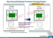
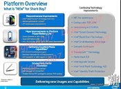
If all goes well with Intel's 22 nm process, Haswell is scheduled for Q2 2013. 2012 (Q2 onwards) will be led by Ivy Bridge. But then here's a "shocker": Haswell's desktop version will use a brand new socket, LGA1150, and will be incompatible with LGA1155. This is because of drastic changes in the pin map of the package. Sandy Bridge and Ivy Bridge share the LGA1155 socket, and will hence, have kept the socket alive for over 2 years. A major change with the component arrangement in the platform that is affecting Haswell's pin map is that Haswell will have a higher bandwidth chipset bus, rearranged PCIe pins (with FDI pins), rearranged power pins, and miscellaneous pins. It does away with a separate power domain for the integrated graphics controller.Haswell will bring several new features to the table, including next-generation RapidStart quick boot capabilities that reduce cold-boot times to 2 seconds. The processor's IPC will be increased over Ivy Bridge. The mobile version will include features that will further increase battery life of mainstream notebooks. Haswell will feature improved media HD to HD transcoding capabilities. It will bring technologies such as NFC (near-field communication), and Thunderbolt (10 Gbps interconnect) to the masses.
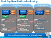
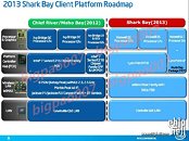
Moving on to the platform itself, it is named "Shark Bay", and will be available in 2-chip quad-core and 1-chip dual-core variants. The quad-core chips and some dual-core chips will use the usual socketed motherboards with a single-chip chipset (PCH) which is smaller than today's PCH chips, while the some dual-core chips will completely integrate the PCH into the processor's package, eliminating an external chipset. The dual-core chips will be available in BGA packages.
Source:
ChipHell
If all goes well with Intel's 22 nm process, Haswell is scheduled for Q2 2013. 2012 (Q2 onwards) will be led by Ivy Bridge. But then here's a "shocker": Haswell's desktop version will use a brand new socket, LGA1150, and will be incompatible with LGA1155. This is because of drastic changes in the pin map of the package. Sandy Bridge and Ivy Bridge share the LGA1155 socket, and will hence, have kept the socket alive for over 2 years. A major change with the component arrangement in the platform that is affecting Haswell's pin map is that Haswell will have a higher bandwidth chipset bus, rearranged PCIe pins (with FDI pins), rearranged power pins, and miscellaneous pins. It does away with a separate power domain for the integrated graphics controller.Haswell will bring several new features to the table, including next-generation RapidStart quick boot capabilities that reduce cold-boot times to 2 seconds. The processor's IPC will be increased over Ivy Bridge. The mobile version will include features that will further increase battery life of mainstream notebooks. Haswell will feature improved media HD to HD transcoding capabilities. It will bring technologies such as NFC (near-field communication), and Thunderbolt (10 Gbps interconnect) to the masses.
Moving on to the platform itself, it is named "Shark Bay", and will be available in 2-chip quad-core and 1-chip dual-core variants. The quad-core chips and some dual-core chips will use the usual socketed motherboards with a single-chip chipset (PCH) which is smaller than today's PCH chips, while the some dual-core chips will completely integrate the PCH into the processor's package, eliminating an external chipset. The dual-core chips will be available in BGA packages.


69 Comments on All's Well That Haswell?
I don't mind the change in motherboards required for a new architecture, as compatibility often puts constraints on performance and compatibility.
It's defitnitely a deliberate way to make people upgrade their entire system rather than just one part.
EDIT: Of course there is the cost incurred on partners who have to develop and engineer new motherboards.
"makes the screen run some funny windows program." Excellent, love it. :D
and we the elite don't care, even better, we love to change'em moar and moar, we have spare time and money to burn haha
no seriously: mobos are of the few parts that still contain excitement and evolution!
Nobody forces us to buy a new platform - it's a freedom we get to choose. There really is no point trying to pin your product evolution on the premise that we must please our users (especially if that premise holds back our development). If we've pleased our users enough, then the product they've got should last comfortably for more than two years.
Upgrading is a choice, not an obligation.
I still have ASrock 775Dual-VSTA motherboard with VIA PT880 chipset that was made for Pentium 4/Pentium D. It works with at least 4 generations of CPUs. From 90nm Pentium 4 to 45nm Core 2 Duo. Got both DDR1/DDR2 and AGP/PCIe support too.
I remember a few years ago there was this big hoo haa over by the time 2012 hits, we'll be seeing up to 32 core cpus - granted this was just a prediction. If competition was as fierce as it was back then, then i suppose we probably could have seen an increase to at least 20+ cores. Since then though we've all found out that by simply slapping on more cores is no good either...coughbulldozercough.