News Posts matching #Hybrid Memory Cube

Return to Keyword Browsing

Micron to Launch HBM2 Memory This Year

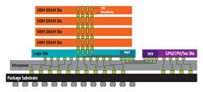
Micron Technologies, in the latest earnings report, announced that they will start shipping High-Bandwidth Memory 2 (HBM2) DRAM. Used for high-performance graphics cards, server processors and all kinds of processors, HBM2 memory is wanted and relatively expensive solution, however, when Micron enters the market of its manufacturing, prices, and the market should adjust for the new player. Previously, only SK-Hynix and Samsung were manufacturing the HBM2 DRAM, however, Micron will join them and they will again form a "big-three" pact that dominates the memory market.

Up until now, Micron used to lay all hopes on its proprietary Hybrid Memory Cube (HMC) DRAM type, which didn't gain much traction from customers and it never really took off. Only a few rare products used it, as Fujitsu SPARC64 XIfx CPU used in Fujitsu PRIMEHPC FX100 supercomputer introduced in 2015. Micron announced to suspend works on HMC in 2018 and decided to devote their efforts to GDDR6 and HBM development. So, as a result, we are seeing that they will launch HBM2 DRAM products sometime this year.
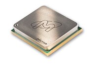
Micron HMC High-Bandwidth Memory

Micron Collaborates With Intel to Enhance "Knights Landing"

Micron Technology, Inc. (Nasdaq:MU), one of the world's leading providers of advanced semiconductor solutions, today announced an ongoing collaboration with Intel to deliver an on-package memory solution for Intel's next-generation Xeon Phi processor, codenamed Knights Landing. The memory solution is the result of a long-term effort between the two companies to break down the memory wall, leveraging the fundamental DRAM and stacking technologies also found in Micron's Hybrid Memory Cube products.

"The ecosystem is changing and the importance of scalable on-package memory and memory bandwidth is now coming to light," said Chirag Dekate, Research Manager at IDC. "Memory is at the heart of the solution space which will benefit both big compute and big data. This announcement is a clear validation of how Micron is advancing the role and impact of memory on systems and the value that 3D memory can deliver."

Micron Technology Licenses Avago Technologies' 30G SerDes for Hybrid Memory Cube

Avago Technologies, a leading supplier of analog interface components for wireless, wireline, and industrial applications, today announced that Micron Technology, Inc. (NASDAQ: MU) has licensed Avago's 28nm Low Power 30Gbps Serializer/Deserializer (SerDes) IP for use in Micron's next generation Hybrid Memory Cube (HMC) devices.

"Avago is an established leader in the development and delivery of high-speed SerDes cores with an offering that is very well suited for integration into our HMC product line," said Tom Eby, vice president of Micron's Compute and Networking Business Unit. "Based on its advanced performance and low power, we are confident that our customers will benefit from the presence of the Avago SerDes on both sides of the memory channel."

Hybrid Memory Cube Consortium Releases HMC 2.0 Specification

The Hybrid Memory Cube Consortium (HMCC), dedicated to the development and establishment of an industry-standard interface specification for the Hybrid Memory Cube (HMC) technology, today announced its continued work to build the HMC ecosystem and support for the industry adoption of this groundbreaking technology through the development of a new interface specification. Today the HMCC also released a first draft of the new specification to a growing list of consortium adopters that now numbers more than 120. The new specification supports increased data rate speeds advancing short-reach (SR) performance from 10 Gb/s, 12.5 Gb/s, and 15 Gb/s, up to 30 Gb/s. The new specification also migrates the associated channel model from SR to VSR to align with existing industry nomenclature. The ultra short-reach (USR) definition also increases performance from 10 Gb/s up to 15 Gb/s.

The HMCC, founded by leading memory providers Micron Technology (Nasdaq:MU), Samsung Electronics, and SK hynix, has begun circulating this draft specification to a broad range of adopters, with the goal of incorporating adopter members' input and targeting a completion date of May 2014 for the final version. The first-generation specification was completed and released publicly in April 2013; several developer and adopter companies, including Altera, Xilinx, and Open-Silicon, have already begun leveraging the specification to design products and solutions that incorporate HMC technology.

Micron Technology Ships First Samples of Hybrid Memory Cube

Micron Technology, Inc., announced today that it is shipping 2GB Hybrid Memory Cube (HMC) engineering samples. HMC represents a dramatic step forward in memory technology, and these engineering samples are the world's first HMC devices to be shared broadly with lead customers. HMC is designed for applications requiring high-bandwidth access to memory, including data packet processing, data packet buffering or storage, and computing applications such as processor accelerators. Micron expects future generations of HMC to migrate to consumer applications within three to five years.

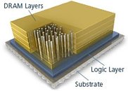
An industry breakthrough, HMC uses advanced through-silicon vias (TSVs)-vertical conduits that electrically connect a stack of individual chips-to combine high-performance logic with Micron's state-of-the-art DRAM. Micron's HMC features a 2GB memory cube that is composed of a stack of four 4Gb DRAM die. The solution provides an unprecedented 160 GB/s of memory bandwidth while using up to 70 percent less energy per bit than existing technologies, which dramatically lowers customers' total cost of ownership (TCO).

Altera and Micron Lead Industry with FPGA & Hybrid Memory Cube Interoperability

Altera Corporation and Micron Technology, Inc. today announced they have jointly demonstrated successful interoperability between Altera Stratix V FPGAs and Micron's Hybrid Memory Cube (HMC). This technology achievement enables system designers to evaluate today the benefits of HMC with FPGAs and SoCs for next-generation communications and high-performance computing designs. The demonstration provides an early proof point that production support of HMC will be delivered with Altera's Generation 10 portfolio, in alignment with market timing, and includes both Stratix 10 and Arria 10 FPGAs and SoCs.

HMC has been recognized by industry leaders and influencers as the long-awaited answer to address the limitations imposed by conventional memory technology, and provides ultra-high system performance with significantly lower power-per-bit. HMC delivers up to 15 times the bandwidth of a DDR3 module and uses 70 percent less energy and 90 percent less space than existing technologies. HMC's abstracted memory allows designers to devote more time leveraging HMC's revolutionary features and performance and less time navigating the multitude of memory parameters required to implement basic functions. It also manages error correction, resiliency, refresh, and other parameters exacerbated by memory process variation. Micron expects to begin sampling HMC later this year with volume production ramping in 2014.

Hybrid Memory Cube Consortium Finalizes Specifications

More than 100 developer and adopter members of the Hybrid Memory Cube Consortium (HMCC) today announced they've reached consensus for the global standard that will deliver a much-anticipated, disruptive memory computing solution. Developed in only 17 months, the final specification marks the turning point for designers in a wide range of segments-from networking and high-performance computing, to industrial and beyond-to begin designing Hybrid Memory Cube (HMC) technology into future products.

A major breakthrough with HMC is the long-awaited utilization of advanced technologies to combine highperformance logic with state-of-the-art DRAM. With this first HMC milestone reached so quickly, consortium members have elected to extend their collaborative effort to achieve agreement on the next generation of HMC interface standards.

Microsoft Joins Hybrid Memory Cube Consortium

The Hybrid Memory Cube Consortium (HMCC), led by Micron Technology, Inc., and Samsung Electronics Co., Ltd., today announced that Microsoft Corp. has joined the consortium. The HMCC is a collaboration of original equipment manufacturers (OEMs), enablers and integrators who are cooperating to develop and implement an open interface standard for an innovative new memory technology called the Hybrid Memory Cube (HMC). Micron and Samsung, the initial developing members of the HMCC, are working closely with Altera, IBM, Open-Silicon, Xilinx and now Microsoft to accelerate widespread industry adoption of HMC technology.

The technology will enable highly efficient memory solutions for applications ranging from industrial products to high-performance computing and large-scale networking. The HMCC's team of developers plans to deliver a draft interface specification to a growing number of "adopters" that are joining the consortium. Then, the combined team of developers and adopters will refine the draft and release a final interface specification at the end of this year.

DDR4 May Use 3D Stacking Technology

Micron Technology, one of the biggest DRAM companies, has announced that it's working the JEDEC standards organization for computer memory, to standardize a new DRAM interface and die-stacking technology called three-dimensional stacking, or 3DS, which may be incorporated into the upcoming DDR4 standard. X-bit labs has a nice summary of how 3DS works:
The idea behind 3DS is to use specially designed and manufactured master-and-slave DRAM die, with only the master die interfacing with the external memory controller. 3DS technology uses optimized DRAM die, single DLL per stack, reduced active logic, single shared external I/O, improved timing, and reduced load to the external world. This combination of features can improve timing, bus speeds, and signal integrity while lowering both power consumption and system overhead for next-generation modules, according to Micron.

IBM to Produce Micron's HMC in Debut of First Commercial, 3D Chip-Making Capability

IBM (NYSE: IBM) and Micron Technology, Inc. announced today that Micron will begin production of a new memory device built using the first commercial CMOS manufacturing technology to employ through-silicon vias (TSVs). IBM's advanced TSV chip-making process enables Micron's Hybrid Memory Cube (HMC) to achieve speeds 15 times faster than today's technology.

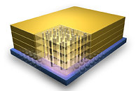
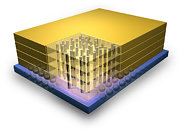
Micron's Hybrid Memory Cube features a stack of individual chips connected by vertical pipelines or "vias," shown above. IBM's new 3-D manufacturing technology, used to connect the 3D micro structure, will be the foundation for commercial production of the new memory cube.

IBM will present the details of its TSV manufacturing breakthrough at the IEEE International Electron Devices Meeting on December 5 in Washington, DC.
Return to Keyword Browsing
Jun 30th, 2024 12:58 EDT change timezone

New Forum Posts

Popular Reviews

Controversial News Posts