News Posts matching #MBCFET

Return to Keyword Browsing

Samsung Foundry Renames 3 nm Process to 2 nm Amid Competition with Intel

In a move that could intensify competition with Intel in the cutting-edge chip manufacturing space, Samsung Foundry has reportedly decided to rebrand its second-generation 3 nm-class fabrication technology, previously known as SF3, to a 2 nm-class manufacturing process called SF2. According to reports from ZDNet, the renaming of Samsung's SF3 to SF2 is likely an attempt by the South Korean tech giant to simplify its process nomenclature and better compete against Intel Foundry, at least visually. Intel is set to roll out its Intel 20A production node, a 2 nm-class technology, later this year. The reports suggest that Samsung has already notified its customers about the changes in its roadmap and the renaming of SF3 to SF2. Significantly, the company has reportedly gone as far as re-signing contracts with customers initially intended to use the SF3 production node.

"We were informed by Samsung Electronics that the 2nd generation 3 nm [name] is being changed to 2 nm," an unnamed source noted to ZDNet. "We had contracted Samsung Foundry for the 2nd generation 3 nm production last year, but we recently revised the contract to change the name to 2 nm." Despite the name change, Samsung's SF3, now called SF2, has not undergone any actual process technology alterations. This suggests that the renaming is primarily a marketing move, as using a different process technology would require customers to rework their chip designs entirely. Samsung intends to start manufacturing chips based on the newly named SF2 process in the second half of 2024. The SF2 technology, which employs gate-all-around (GAA) transistors that Samsung brands as Multi-Bridge-Channel Field Effect Transistors (MBCFET), does not feature a backside power delivery network (BSPDN), a significant advantage of Intel's 20A process. Samsung Foundry has not officially confirmed the renaming.

Samsung Electronics Collaborates with Arm on Optimized Next Gen Cortex-X CPU Using 2nm SF2 GAAFET Process

Samsung Electronics Co., Ltd., a world leader in advanced semiconductor technology, today announced a collaboration to deliver optimized next generation Arm Cortex -X CPU developed on Samsung Foundry's latest Gate-All-Around (GAA) process technology. This initiative is built on years of partnership with millions of devices shipped with Arm CPU intellectual property (IP) on various process nodes offered by Samsung Foundry.

This collaboration sets the stage for a series of announcements and planned innovation between Samsung and Arm. The companies have bold plans to reinvent 2-nanometer (nm) GAA for next-generation data center and infrastructure custom silicon, and a groundbreaking AI chiplet solution that will revolutionize the future generative artificial intelligence (AI) mobile computing market.

Samsung Begins Chip Production Using 3nm Process Technology With GAA Architecture

Samsung Electronics, the world leader in semiconductor technology, today announced that it has started initial production of its 3-nanometer (nm) process node applying Gate-All-Around (GAA) transistor architecture. Multi-Bridge-Channel FET (MBCFET), Samsung's GAA technology implemented for the first time ever, defies the performance limitations of FinFET, improving power efficiency by reducing the supply voltage level, while also enhancing performance by increasing drive current capability. Samsung is starting the first application of the nanosheet transistor with semiconductor chips for high performance, low power computing application and plans to expand to mobile processors.

"Samsung has grown rapidly as we continue to demonstrate leadership in applying next-generation technologies to manufacturing, such as foundry industry's first High-K Metal Gate, FinFET, as well as EUV. We seek to continue this leadership with the world's first 3 nm process with the MBCFET," said Dr. Siyoung Choi, President and Head of Foundry Business at Samsung Electronics. "We will continue active innovation in competitive technology development and build processes that help expedite achieving maturity of technology."

Samsung Foundry Announces GAA Ready, 3nm in 2022, 2nm in 2025, Other Speciality Nodes

Samsung Electronics, a world leader in advanced semiconductor technology, today unveiled plans for continuous process technology migration to 3- and 2-nanometer (nm) based on the company's Gate-All-Around (GAA) transistor structure at its 5th annual Samsung Foundry Forum (SFF) 2021. With a theme of "Adding One More Dimension," the multi-day virtual event is expected to draw over 2,000 global customers and partners. At this year's event, Samsung will share its vision to bolster its leadership in the rapidly evolving foundry market by taking each respective part of foundry business to the next level: process technology, manufacturing operations, and foundry services.

"We will increase our overall production capacity and lead the most advanced technologies while taking silicon scaling a step further and continuing technological innovation by application," said Dr. Siyoung Choi, President and Head of Foundry Business at Samsung Electronics. "Amid further digitalization prompted by the COVID-19 pandemic, our customers and partners will discover the limitless potential of silicon implementation for delivering the right technology at the right time."

Samsung Demonstrates 256 Gb 3 nm MBCFET Chip at ISSCC 2021

During the IEEE International Solid-State Circuits Conference (ISSCC), Samsung Foundry has presented a new step towards smaller and more efficient nodes. The new chip that was presented is a 256 Gb memory chip, based on SRAM technology. However, all of that doesn't sound interesting, until we mention the technology that is behind it. Samsung has for the first time manufactured a chip using the company's gate-all-around field-effect transistor (GAAFET) technology on the 3 nm semiconductor node. Formally, there are two types of GAAFET technology: the regular GAAFET that uses nanowires as fins of the transistor, and MBCFET (multi-bridge channel FET) that uses thicker fins that come in a form of a nanosheet.

Samsung has demonstrated the first SRAM chip that uses MBCFET technology today. The chip in question is a 256 Gb chip with an area of 56 mm². The achievement Samsung is proud of is that the chip uses 230 mV less power for writes, compared to the standard approach, as the MBCFET transistors allow the company to have many different power-saving techniques. The new 3 nm MBCFET process is expected to get into high-volume production sometime in 2022, however, we are yet to see demos of logic chips besides SRAM like we see today. Nonetheless, even the demonstration of SRAM is big progress, and we are eager to see what the company manages to build with the new technology.

TSMC Achieves Major Breakthrough in 2 nm Manufacturing Process, Risk Production in 2023

The Taiwan Economic Daily claims that TSMC has achieved a major internal breakthrough for the eventual rollout of 2 nm fabrication process technology. According to the publication, this breakthrough has turned TSMC even more optimistic towards a 2023 rollout of 2 nm risk production - which is all the more impressive considering reports that TSMC will be leaving the FinFet realm for a new multi-bridge channel field effect transistor (MBCFET) architecture - itself based on the Gate-All-Around (GAA) technology. This breakthrough comes one year after TSMC put together an internal team whose aim was to pave the way for 2 nm deployment.

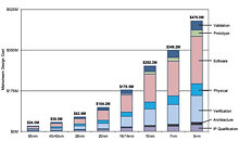
MBCFET expands on the GAAFET architecture by taking the Nanowire field-effect transistor and expanding it so that it becomes a Nanosheet. The main idea is to make the field-effect transistor three-dimensional. This new complementary metal oxide semiconductor transistor can improve circuit control and reduce leakage current. This design philosophy is not exclusive to TSMC - Samsung has plans to deploy a variant of this design on their 3 nm process technology. And as has been the norm, further reductions in chip fabrication scale come at hefty costs - while the development cost for 5 nm has already achieved $476M in cost, Samsung reports that their 3 nm GAA technology will cost in excess of $500M - and 2 nm, naturally, will come in even costlier than that.
Return to Keyword Browsing
Dec 19th, 2024 10:13 EST change timezone

New Forum Posts

Popular Reviews

Controversial News Posts