News Posts matching #Maxwell

Return to Keyword Browsing

GM107 Features 128 CUDA Cores Per Streaming Multiprocessor

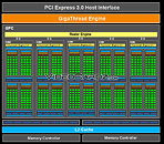
NVIDIA's upcoming GM107 GPU, the first to be based on its next-generation "Maxwell" GPU architecture, reportedly features a different arrangement of CUDA cores and streaming multiprocessors to those typically associated with "Kepler," although the component hierarchy is similar. The chip reportedly features five streaming multiprocessors, highly integrated computation subunits of the GPU. NVIDIA is referring to these parts as "streaming multiprocessor (Maxwell)," or SMMs.

Further, each streaming multiprocessor features 128 CUDA cores, and not the 192 CUDA cores found in SMX units of "Kepler" GPUs. If true, GM107 features 640 CUDA cores, all of which will be enabled on the GeForce GTX 750 Ti. If NVIDIA is carving out the GTX 750 by disabling one of those streaming multiprocessors, its CUDA core count works out to be 512. NVIDIA will apparently build two GPUs on the existing 28 nm process, the GM107, and the smaller GM108; and three higher performing chips on the next-generation 20 nm process, the GM206, the GM204, and the GM200. The three, as you might have figured out, succeed the GK106, GK104, and GK110, respectively.

NVIDIA GM107 "Maxwell" Silicon Pictured

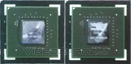
Here is the first picture of a couple of NVIDIA GM107 silicons in a tray, ahead of graphics card assembly. The packages appear to be as big as those of the GK106 from the previous generation, however, the die itself is estimated to be smaller, at roughly 156 mm², compared to the 221 mm² die of the GK106, and the 118 mm² of the GK107. The best part? All three chips are built on the same 28 nm silicon fab process. So what makes the GM107 die smaller than that of the GK106 despite having a similar feature-set? Narrower memory bus. The GM107 is said to feature a 128-bit wide GDDR5 memory interface, in comparison to the 192-bit wide interface of the GK106.

Apart from the 128-bit wide GDDR5 memory interface, the GM107 is said to feature a total of 960 CUDA cores, 80 TMUs, and 16 ROPs. The CUDA core count is identical to that of the GK106. The GM107 is built on NVIDIA's next-generation "Maxwell" GPU architecture. It will form the foundation of two SKUs, the GeForce GTX 750 Ti, and the GeForce GTX 750. The former features the full complement of 960 CUDA cores; while the latter is slightly cut down, and features just 768. The TDP of the GTX 750 Ti is approximated to be around 75 Watt. If true, the GTX 750 duo will set new standards on the performance-per-Watt metrics. NVIDIA is expected to launch both, later this month.

GeForce GTX 750 Ti Benchmarked Some More

In the run up to its rumored February 18th launch, GeForce GTX 750 Ti, the first retail GPU based on NVIDIA's next-generation "Maxwell" GPU architecture, the card is finding itself in the hands of more leaky PC enthusiasts, this time, members of Chinese PC enthusiast community site PCOnline. The site used an early driver to test the GTX 750 Ti, which it put through 3DMark 11 (performance preset) and 3DMark Fire Strike. In the former, the card scored P4188 points, and 3170 points in the latter. The test-bed details are not mentioned, but one can make out a stock Core i7-4770K from one of the screenshots. Also accompanying the two is an alleged GPU-Z 0.7.5 screenshot of the GTX 750 Ti, which reads out its CUDA core count as 960. Version 0.7.5 doesn't support GTX 750 Ti, but it has fall-backs that help it detect unknown GPUs, particularly from NVIDIA. Its successor, GPU-Z 0.7.6, which we're releasing later today, comes with support for the chip.

ASUS GeForce GTX 750 Ti "Maxwell" Sees First Listing

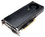
Way ahead of its rumored February 18 launch, a Hungarian online retailer listed an ASUS-branded GeForce GTX 750 Ti graphics card, bearing model number GTX750TI-OC-2GD5. The card is listed at a tax-inclusive price of 50,000 HUF (around US $225), which is rather steep, even for a pre-order, given the positioning of the card, in relation to existing products, such as the GTX 660 and GTX 760. The naming suggests that the card is factory-overclocked, which means that NVIDIA will allow factory-overclocked, and possibly custom design GTX 750 Ti cards from day-one. It also gives away the memory of the card, at 2 GB GDDR5. The listing, however, doesn't go with any pictures.

GeForce GTX 750 Ti "Maxwell" First Performance Numbers Out

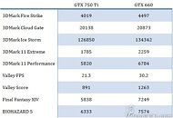
Ahead of its rumored mid-February launch, members of Taiwanese tech forum Coolaler.com posted the first performance benchmark numbers of the card. Originally thought to be positioned between the previous-generation GeForce GTX 660 and current GTX 760, the GTX 750 Ti, according to these numbers is on average 10 to 15 percent slower than the GTX 660, which should put its performance somewhere in between the GTX 650 Ti Boost and the GTX 660.

Then again, the testers must be using some very early drivers, and performance figures of the GTX 750 Ti should get clearer as its mid-February launch date approaches. The GeForce GTX 750 Ti is an important GPU for NVIDIA, as it's the first to be based on its next-generation "Maxwell" GPU micro-architecture. NVIDIA is trying the architecture out on current 28 nm process, before launching bigger chips based on the next-generation 20 nm fab process.

NVIDIA Readies GeForce GTX 750 Ti Based on "Maxwell"

NVIDIA's next-generation GPU architecture, codenamed "Maxwell," will debut this February, with the unexpectedly positioned GeForce GTX 750. The card will launch on February 18, to be specific. Maxwell will introduce a host of new features for NVIDIA, beginning with Unified Virtual Memory. The feature lets the GPU and CPU share the same memory. Such a feature is already implemented on the current CUDA, but Maxwell could be designed to reduce overhead involved in getting the thing to work. The next big feature is that Maxwell GPUs will embed a 64-bit ARM CPU core based on NVIDIA's "Project Denver." This CPU core will allow the GPU to reduce dependency on the system's main processor in certain GPGPU scenarios. Pole-vaulting the CPU's authority in certain scenarios could work to improve performance

Getting back to the GeForce GTX 750 Ti, NVIDIA's aim is simple, to see how "Maxwell" performs on the existing, proven 28 nanometer silicon fab process, before scaling it up on the future 20 nm nodes, with bigger chips. Given its name, we expect it to be positioned in between the GTX 760 and the GTX 660 in terms of gaming performance, but we won't be surprised if it falls into an entirely different league with GPGPU. There are no specifications at hand.

NVIDIA Updates GPU Roadmap with "Volta"

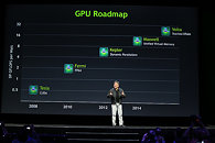
NVIDIA updated its GPU micro-architecture roadmap at the 2013 GPU Technology Conference (GTC). Currently spearheaded by the "Kepler" micro-architecture, which drives its GeForce, Quadro, and Tesla product lines, and which will drive Tegra mobile SoCs in 2014; NVIDIA's next-generation "Maxwell" could make its debut some time in 2014. Going by NVIDIA's graph that puts performance-per-Watt against time, "Maxwell" should nearly double performance. Maxwell GPUs feature unified virtual memory, which lets CPUs treat graphics card memory as system memory, for faster general-purpose performance.

Although not backed by a tentative launch year, and assuming "Maxwell" has its run for another two years, 2016 could see the launch of NVIDIA's "Volta" GPU micro-architecture. In addition to advancements by its predecessors, "Volta" could introduce stacked DRAM technology. It would enable GPU memory bandwidths as high as 1 TB/s. Current high-end graphics cards such as GeForce Titan and Radeon HD 7970 GHz Edition, are capable of breaching the 300 GB/s mark, so NVIDIA's claims don't sound far-fetched.
Return to Keyword Browsing
Dec 3rd, 2024 13:37 EST change timezone

New Forum Posts

Popular Reviews

Controversial News Posts