News Posts matching #Milan

Return to Keyword Browsing

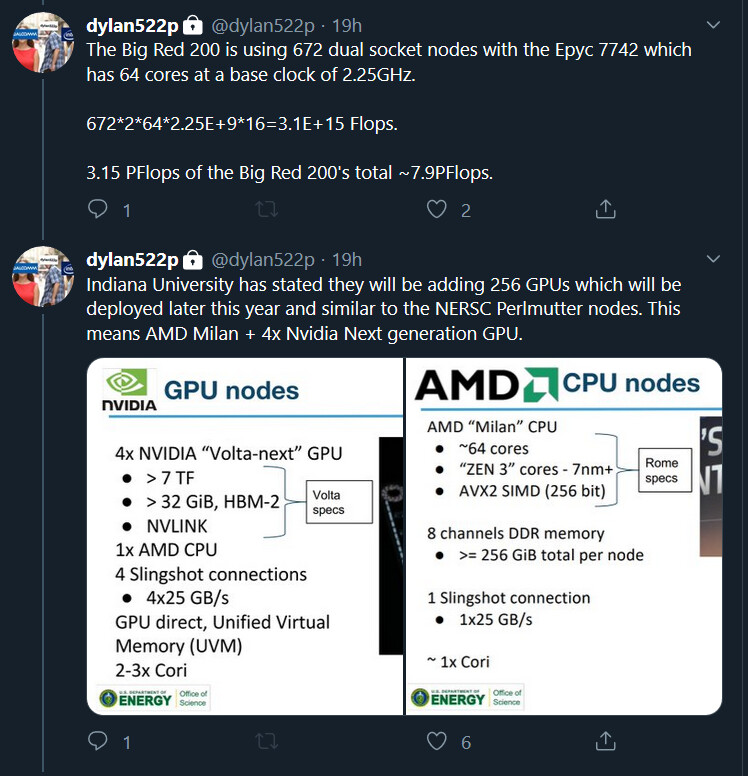
NERSC Finalizes Contract for Perlmutter Supercomputer Powered by AMD Milan and NVIDIA Volta-Successor

The National Energy Research Scientific Computing Center (NERSC), the mission high-performance computing facility for the U.S. Department of Energy's Office of Science, has moved another step closer to making Perlmutter - its next-generation GPU-accelerated supercomputer - available to the science community in 2020.

In mid-April, NERSC finalized its contract with Cray - which was acquired by Hewlett Packard Enterprise (HPE) in September 2019 - for the new system, a Cray Shasta supercomputer that will feature 24 cabinets and provide 3-4 times the capability of NERSC's current supercomputer, Cori. Perlmutter will be deployed at NERSC in two phases: the first set of 12 cabinets, featuring GPU-accelerated nodes, will arrive in late 2020; the second set, featuring CPU-only nodes, will arrive in mid-2021. A 35-petabyte all-flash Lustre-based file system using HPE's ClusterStor E1000 hardware will also be deployed in late 2020.

AMD Confirms Zen 3 and RDNA2 by Late-2020

AMD in its post Q1-2020 earnings release disclosures stated that the company is "on track" to launching its next-generation "Zen 3" CPU microarchitecture and RDNA2 graphics architecture in late-2020. The company did not reveal in what shape or form the two will debut. AMD is readying "Zen 3" based EPYC "Milan" enterprise processors, "Vermeer" Ryzen desktop processors, and "Cezanne" Ryzen mobile APUs based on "Zen 3," although there's no word on which product line the microarchitecture will debut with. "Zen 3" compute dies (CCDs) are expected to do away with the quad-core compute complex (CCX) arrangement of cores, and are expected to be built on a refined 7 nm-class silicon fabrication process, either TSMC N7P or N7+.

The only confirmed RDNA2 based products we have as of now are the semi-custom SoCs that drive the Sony PlayStation 5 and Microsoft Xbox Series X next-generation consoles, which are expected to debut by late-2020. The AMD tweet, however, specifies "GPUs" (possibly referring to discrete GPUs). Also, with AMD forking its graphics IP to RDNA (for graphics processors) and CDNA (for headless compute accelerators), we're fairly sure AMD is referring to a Radeon RX or Radeon Pro launch in the tweet. Microsoft's announcement of the DirectX 12 Ultimate logo is expected to expedite launch of Radeon RX discrete GPUs based on RDNA2, as the current RDNA architecture doesn't meet the logo requirements.

AMD Financial Analyst Day 2020 Live Blog

AMD Financial Analyst Day presents an opportunity for AMD to talk straight with the finance industry about the company's current financial health, and a taste of what's to come. Guidance and product teasers made during this time are usually very accurate due to the nature of the audience. In this live blog, we will post information from the Financial Analyst Day 2020 as it unfolds.
20:59 UTC: The event has started as of 1 PM PST. CEO Dr Lisa Su takes stage.

NVIDIA's Next-Generation "Ampere" GPUs Could Have 18 TeraFLOPs of Compute Performance

NVIDIA will soon launch its next-generation lineup of graphics cards based on a new and improved "Ampere" architecture. With the first Tesla server cards that are a part of the Ampere lineup going inside Indiana University Big Red 200 supercomputer, we now have some potential specifications and information about its compute performance. Thanks to the Twitter user dylan552p(@dylan522p), who did some math about the potential compute performance of the Ampere GPUs based on NextPlatform's report, we discovered that Ampere is potentially going to feature up to 18 TeraFLOPs of FP64 compute performance.

With Big Red 200 supercomputer being based on Cray's Shasta supercomputer building block, it is being deployed in two phases. The first phase is the deployment of 672 dual-socket nodes powered by AMD's EPYC 7742 "Rome" processors. These CPUs provide 3.15 PetaFLOPs of combined FP64 performance. With a total of 8 PetaFLOPs planned to be achieved by the Big Red 200, that leaves just a bit under 5 PetaFLOPs to be had using GPU+CPU enabled system. Considering the configuration of a node that contains one next-generation AMD "Milan" 64 core CPU, and four of NVIDIA's "Ampere" GPUs alongside it. If we take for a fact that Milan boosts FP64 performance by 25% compared to Rome, then the math shows that the 256 GPUs that will be delivered in the second phase of Big Red 200 deployment will feature up to 18 TeraFLOPs of FP64 compute performance. Even if "Milan" doubles the FP64 compute power of "Rome", there will be around 17.6 TeraFLOPs of FP64 performance for the GPU.

AMD CEO To Unveil "Zen 3" Microarchitecture at CES 2020

A prominent Taiwanese newspaper reported that AMD will formally unveil its next-generation "Zen 3" CPU microarchitecture at the 2020 International CES. Company CEO Dr Lisa Su will head an address revealing three key client-segment products under the new 4th generation Ryzen processor family, and the company's 3rd generation EPYC enterprise processor family based on the "Milan" MCM that succeeds "Rome." AMD is keen on developing an HEDT version of "Milan" for the 4th generation Ryzen Threadripper family, codenamed "Genesis Peak."

The bulk of the client-segment will be addressed by two distinct developments, "Vermeer" and "Renoir." The "Vermeer" processor is a client-desktop MCM that succeeds "Matisse," and will implement "Zen 3" chiplets. "Renoir," on the other hand, is expected to be a monolithic APU that combines "Zen 2" CPU cores with an iGPU based on the "Vega" graphics architecture, with updated display- and multimedia-engines from "Navi." The common thread between "Milan," "Genesis Peak," and "Vermeer" is the "Zen 3" chiplet, which AMD will build on the new 7 nm EUV silicon fabrication process at TSMC. AMD stated that "Zen 3" will have IPC increases in line with a new microarchitecture.

AMD Zen 3 Could Bid the CCX Farewell, Feature Updated SMT

With its next-generation "Zen 3" CPU microarchitecture designed for the 7 nm EUV silicon fabrication process, AMD could bid the "Zen" compute complex or CCX farewell, heralding chiplets with monolithic last-level caches (L3 caches) that are shared across all cores on the chiplet. AMD embraced a quad-core compute complex approach to building multi-core processors with "Zen." At the time, the 8-core "Zeppelin" die featured two CCX with four cores, each. With "Zen 2," AMD reduced the CPU chiplet to only containing CPU cores, L3 cache, and an Infinity Fabric interface, talking to an I/O controller die elsewhere on the processor package. This reduces the economic or technical utility in retaining the CCX topology, which limits the amount of L3 cache individual cores can access.

This and more juicy details about "Zen 3" were put out by a leaked (later deleted) technical presentation by company CTO Mark Papermaster. On the EPYC side of things, AMD's design efforts will be spearheaded by the "Milan" multi-chip module, featuring up to 64 cores spread across eight 8-core chiplets. Papermaster talked about how the individual chiplets will feature "unified" 32 MB of last-level cache, which means a deprecation of the CCX topology. He also detailed an updated SMT implementation that doubles the number of logical processors per physical core. The I/O interface of "Milan" will retain PCI-Express gen 4.0 and eight-channel DDR4 memory interface.
Return to Keyword Browsing
Jul 1st, 2025 02:36 CDT change timezone

New Forum Posts

Popular Reviews

TPU on YouTube

Controversial News Posts