Mar 31st, 2025 05:22 EDT
change timezone
Latest GPU Drivers
New Forum Posts
- Technical Issues - TPU Main Site & Forum (2025) (82)
- Can you guess Which game it is? (36)
- Windows 10 Vs 11, Which one too choose? (129)
- The TPU UK Clubhouse (26016)
- 5070 Ti power limit questions (26)
- Your PC ATM (35311)
- Future-proofing my OLED (83)
- AMD RX 9070 XT & RX 9070 non-XT thread (OC, undervolt, benchmarks, ...) (72)
- Free Games Thread (4604)
- 7900 XTX Cyberpunk RT (3)
Popular Reviews
- Sapphire Radeon RX 9070 XT Pulse Review
- ASRock Phantom Gaming B850 Riptide Wi-Fi Review - Amazing Price/Performance
- Samsung 9100 Pro 2 TB Review - The Best Gen 5 SSD
- Palit GeForce RTX 5070 GamingPro OC Review
- Sapphire Radeon RX 9070 XT Nitro+ Review - Beating NVIDIA
- Assassin's Creed Shadows Performance Benchmark Review - 30 GPUs Compared
- Enermax REVOLUTION D.F. 12 850 W Review
- AMD Ryzen 7 9800X3D Review - The Best Gaming Processor
- ASRock Radeon RX 9070 XT Taichi OC Review - Excellent Cooling
- XPG LEVANTE II 360 Review
Controversial News Posts
- AMD RDNA 4 and Radeon RX 9070 Series Unveiled: $549 & $599 (260)
- MSI Doesn't Plan Radeon RX 9000 Series GPUs, Skips AMD RDNA 4 Generation Entirely (142)
- Microsoft Introduces Copilot for Gaming (124)
- AMD Radeon RX 9070 XT Reportedly Outperforms RTX 5080 Through Undervolting (119)
- NVIDIA Reportedly Prepares GeForce RTX 5060 and RTX 5060 Ti Unveil Tomorrow (115)
- Over 200,000 Sold Radeon RX 9070 and RX 9070 XT GPUs? AMD Says No Number was Given (100)
- NVIDIA GeForce RTX 5050, RTX 5060, and RTX 5060 Ti Specifications Leak (96)
- Retailers Anticipate Increased Radeon RX 9070 Series Prices, After Initial Shipments of "MSRP" Models (90)
News Posts matching #N4X
Return to Keyword Browsing
AMD to Reduce RDNA 4 "Navi 44" Chip Package Size
GPU chip packages of the "Navi 4x" generation of GPUs could be generationally smaller than their predecessors, according to leaked package dimensions of the "Navi 44" chip put out by Olrak29_. With its next-generation Radeon RX gaming GPUs based on the RDNA 4 graphics architecture, AMD has decided to focus on gaining market-share in the performance and mainstream segments, ceding the enthusiast segment to NVIDIA. As part of its effort, the company is making RDNA 4 efficient at every level—architecture, process, and package.
At the architecture level, RDNA 4 is expected to improve performance, particularly the performance cost of ray tracing, through a more specialized ray tracing hardware stack. At the process level, AMD is expected to switch to a more efficient foundry node, with some reports suggesting the TSMC 4 nm, such as the N4P or N4X. For a mid-range GPU like the "Navi 44," which succeeds the "Navi 23" and "Navi 33," these mean a rather big leap from the 7 nm or 6 nm DUV nodes. The leak suggests a smaller package, measuring 29 mm x 29 mm. In comparison, the "Navi 23" package measures 35 mm x 35 mm. The smaller package could make these GPUs friendlier with gaming notebooks, where mainboard PCB real-estate is at a premium.
At the architecture level, RDNA 4 is expected to improve performance, particularly the performance cost of ray tracing, through a more specialized ray tracing hardware stack. At the process level, AMD is expected to switch to a more efficient foundry node, with some reports suggesting the TSMC 4 nm, such as the N4P or N4X. For a mid-range GPU like the "Navi 44," which succeeds the "Navi 23" and "Navi 33," these mean a rather big leap from the 7 nm or 6 nm DUV nodes. The leak suggests a smaller package, measuring 29 mm x 29 mm. In comparison, the "Navi 23" package measures 35 mm x 35 mm. The smaller package could make these GPUs friendlier with gaming notebooks, where mainboard PCB real-estate is at a premium.


Ryzen 9000 Chip Layout: New Details Announced
AMD "Granite Ridge" is codename for the four new Ryzen 9000 series desktop processors the company plans to launch on July 31, 2024. The processor is built in the Socket AM5 package, and is meant to be backwards compatible with AMD 600-series chipset motherboards, besides the new 800-series chipset ones that will launch alongside. "Granite Ridge" is a chiplet-based processor, much like the Ryzen 7000 "Raphael," Ryzen 5000 "Vermeer," and Ryzen 3000 "Matisse." AMD is carrying over the 6 nm client I/O die over from "Raphael" in an effort to minimize development costs, much in the same way it carried over the 12 nm cIOD for "Vermeer" from "Matisse."
The SoC I/O features of "Granite Ridge" are contemporary, with its awesome 28-lane PCI-Express Gen 5 root complex that allows a PCI-Express 5.0 x16, two CPU-attached M.2 Gen 5 slots, and a Gen 5 x4 chipset bus. There's also a basic integrated graphics solution based on the older RDNA 2 graphics architecture; which should make these processors fit for all use-cases that don't need discrete graphics. The iGPU even has multimedia accelerators, an audio coprocessor, a display controller, and USB 3.2 interfaces from the processor.


The SoC I/O features of "Granite Ridge" are contemporary, with its awesome 28-lane PCI-Express Gen 5 root complex that allows a PCI-Express 5.0 x16, two CPU-attached M.2 Gen 5 slots, and a Gen 5 x4 chipset bus. There's also a basic integrated graphics solution based on the older RDNA 2 graphics architecture; which should make these processors fit for all use-cases that don't need discrete graphics. The iGPU even has multimedia accelerators, an audio coprocessor, a display controller, and USB 3.2 interfaces from the processor.
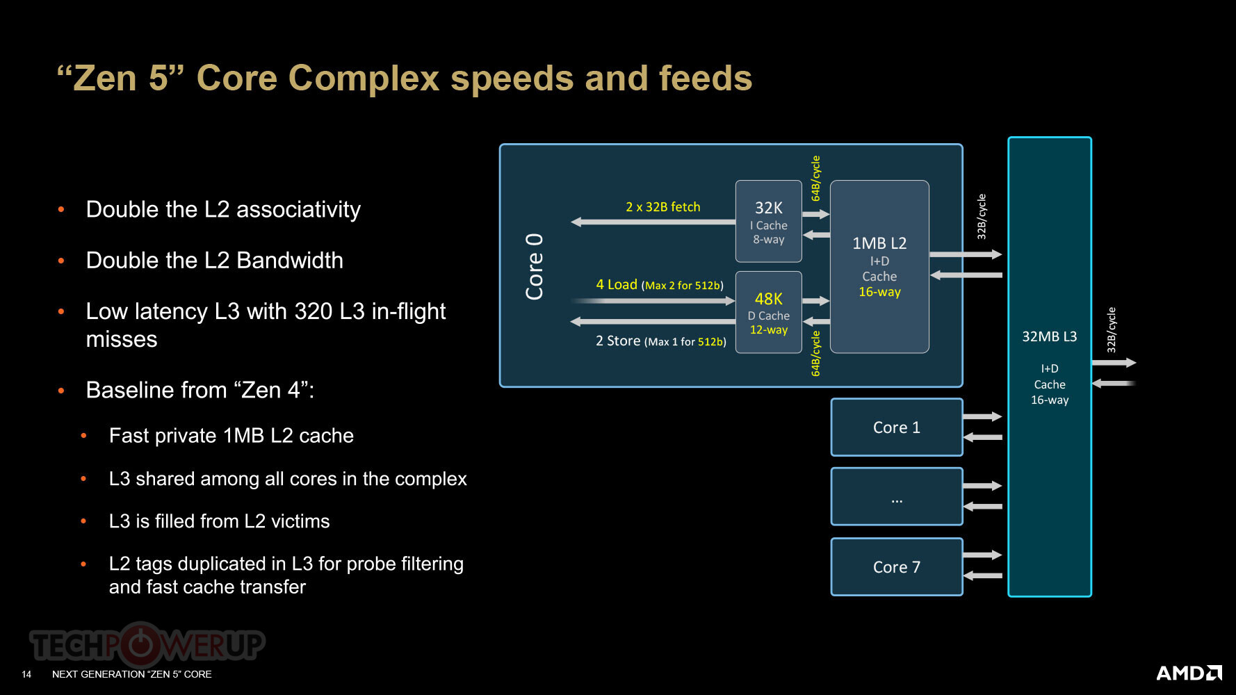


AMD Granite Ridge and Strix Point Zen 5 Die-sizes and Transistor Counts Confirmed
AMD is about give the new "Zen 5" microarchitecture a near-simultaneous launch across both its client segments—desktop and mobile. The desktop front is held by the Ryzen 9000 "Granite Ridge" Socket AM5 processors; while Ryzen AI 300 "Strix Point" powers the company's crucial effort to capture Microsoft Copilot+ AI PC market share. We recently did a technical deep-dive on the two. HardwareLuxx.de scored two important bits of specs for both processors in its Q&A interaction with AMD—die sizes and transistor counts.
To begin with, "Strix Point" is a monolithic silicon, which is confirmed to be built on the TSMC N4P foundry node (4 nm). This is a slight upgrade over the N4 node that the company built its previous generation "Phoenix" and "Hawk Point" processors on. The "Strix Point" silicon measures 232.5 mm² in area, which is significantly larger than the 178 mm² of "Hawk Point" and "Phoenix." The added die area comes from there being 12 CPU cores instead of 8, and 16 iGPU compute units instead of 12; and a larger NPU. There are many other factors, such as the larger 24 MB CPU L3 cache; and the sizes of the "Zen 5" and "Zen 5c" cores themselves.

To begin with, "Strix Point" is a monolithic silicon, which is confirmed to be built on the TSMC N4P foundry node (4 nm). This is a slight upgrade over the N4 node that the company built its previous generation "Phoenix" and "Hawk Point" processors on. The "Strix Point" silicon measures 232.5 mm² in area, which is significantly larger than the 178 mm² of "Hawk Point" and "Phoenix." The added die area comes from there being 12 CPU cores instead of 8, and 16 iGPU compute units instead of 12; and a larger NPU. There are many other factors, such as the larger 24 MB CPU L3 cache; and the sizes of the "Zen 5" and "Zen 5c" cores themselves.


TSMC Ramps up Shipments to Record Levels, 5/4 nm Production Lines at Capacity
According to DigiTimes, TSMC is working on increased its monthly shipments of finished wafers from 120,000 to 150,000 for its 5 nm nodes, under which 4 nm also falls. This is three times as much as what TSMC was producing just a year ago. The 4 nm node is said to be in full mass production now and the enhanced N4P node should be ready for mass production in the second half of 2022, alongside N3B. This will be followed by the N4X and N3E nodes in 2023. The N3B node is expected to hit 40-50,000 wafers initially, before ramping up from there, assuming everything is on track.
The report also mentions that TSMC is expecting a 20 percent revenue increase from its 28 to 7 nm nodes this year, which shows that even these older nodes are being heavily utilised by its customers. TSMC has what NVIDIA would call a demand problem, as the company simply can't meet demand at the moment, with customers lining up to be able to get a share of any additional production capacity. NVIDIA is said to have paid TSMC at least US$10 billion in advance to secure manufacturing capacity for its upcoming products, both for consumer and enterprise products. TSMC's top three HPC customers are also said to have pre-booked capacity on the upcoming 3 and 2 nm nodes, so it doesn't look like demand is going to ease up anytime soon.
The report also mentions that TSMC is expecting a 20 percent revenue increase from its 28 to 7 nm nodes this year, which shows that even these older nodes are being heavily utilised by its customers. TSMC has what NVIDIA would call a demand problem, as the company simply can't meet demand at the moment, with customers lining up to be able to get a share of any additional production capacity. NVIDIA is said to have paid TSMC at least US$10 billion in advance to secure manufacturing capacity for its upcoming products, both for consumer and enterprise products. TSMC's top three HPC customers are also said to have pre-booked capacity on the upcoming 3 and 2 nm nodes, so it doesn't look like demand is going to ease up anytime soon.

TSMC Announces the N4X Silicon Fabrication Process
TSMC today introduced its N4X process technology, tailored for the demanding workloads of high performance computing (HPC) products. N4X is the first of TSMC's HPC-focused technology offerings, representing ultimate performance and maximum clock frequencies in the 5-nanometer family. The "X" designation is reserved for TSMC technologies that are developed specifically for HPC products.
"HPC is now TSMC's fastest-growing business segment and we are proud to introduce N4X, the first in the 'X' lineage of our extreme performance semiconductor technologies," said Dr. Kevin Zhang, senior vice president of Business Development at TSMC. "The demands of the HPC segment are unrelenting, and TSMC has not only tailored our 'X' semiconductor technologies to unleash ultimate performance but has also combined it with our 3DFabric advanced packaging technologies to offer the best HPC platform."
"HPC is now TSMC's fastest-growing business segment and we are proud to introduce N4X, the first in the 'X' lineage of our extreme performance semiconductor technologies," said Dr. Kevin Zhang, senior vice president of Business Development at TSMC. "The demands of the HPC segment are unrelenting, and TSMC has not only tailored our 'X' semiconductor technologies to unleash ultimate performance but has also combined it with our 3DFabric advanced packaging technologies to offer the best HPC platform."
Mar 31st, 2025 05:22 EDT
change timezone
Latest GPU Drivers
New Forum Posts
- Technical Issues - TPU Main Site & Forum (2025) (82)
- Can you guess Which game it is? (36)
- Windows 10 Vs 11, Which one too choose? (129)
- The TPU UK Clubhouse (26016)
- 5070 Ti power limit questions (26)
- Your PC ATM (35311)
- Future-proofing my OLED (83)
- AMD RX 9070 XT & RX 9070 non-XT thread (OC, undervolt, benchmarks, ...) (72)
- Free Games Thread (4604)
- 7900 XTX Cyberpunk RT (3)
Popular Reviews
- Sapphire Radeon RX 9070 XT Pulse Review
- ASRock Phantom Gaming B850 Riptide Wi-Fi Review - Amazing Price/Performance
- Samsung 9100 Pro 2 TB Review - The Best Gen 5 SSD
- Palit GeForce RTX 5070 GamingPro OC Review
- Sapphire Radeon RX 9070 XT Nitro+ Review - Beating NVIDIA
- Assassin's Creed Shadows Performance Benchmark Review - 30 GPUs Compared
- Enermax REVOLUTION D.F. 12 850 W Review
- AMD Ryzen 7 9800X3D Review - The Best Gaming Processor
- ASRock Radeon RX 9070 XT Taichi OC Review - Excellent Cooling
- XPG LEVANTE II 360 Review
Controversial News Posts
- AMD RDNA 4 and Radeon RX 9070 Series Unveiled: $549 & $599 (260)
- MSI Doesn't Plan Radeon RX 9000 Series GPUs, Skips AMD RDNA 4 Generation Entirely (142)
- Microsoft Introduces Copilot for Gaming (124)
- AMD Radeon RX 9070 XT Reportedly Outperforms RTX 5080 Through Undervolting (119)
- NVIDIA Reportedly Prepares GeForce RTX 5060 and RTX 5060 Ti Unveil Tomorrow (115)
- Over 200,000 Sold Radeon RX 9070 and RX 9070 XT GPUs? AMD Says No Number was Given (100)
- NVIDIA GeForce RTX 5050, RTX 5060, and RTX 5060 Ti Specifications Leak (96)
- Retailers Anticipate Increased Radeon RX 9070 Series Prices, After Initial Shipments of "MSRP" Models (90)