News Posts matching #OpenCL

Return to Keyword Browsing

NVIDIA MX550 Rumored to Feature GA107 GPU with 2 GB of GDDR6 memory

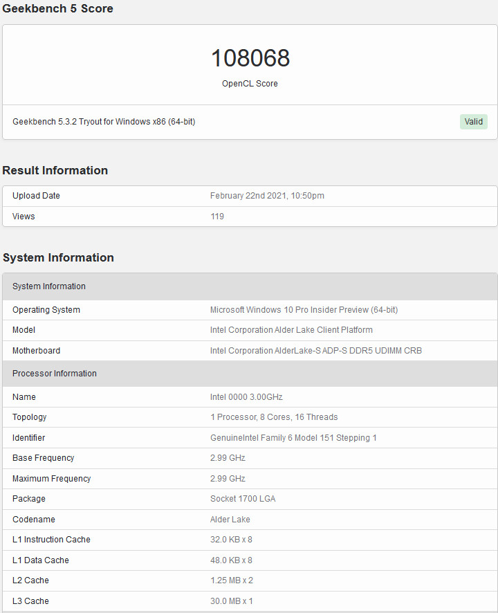
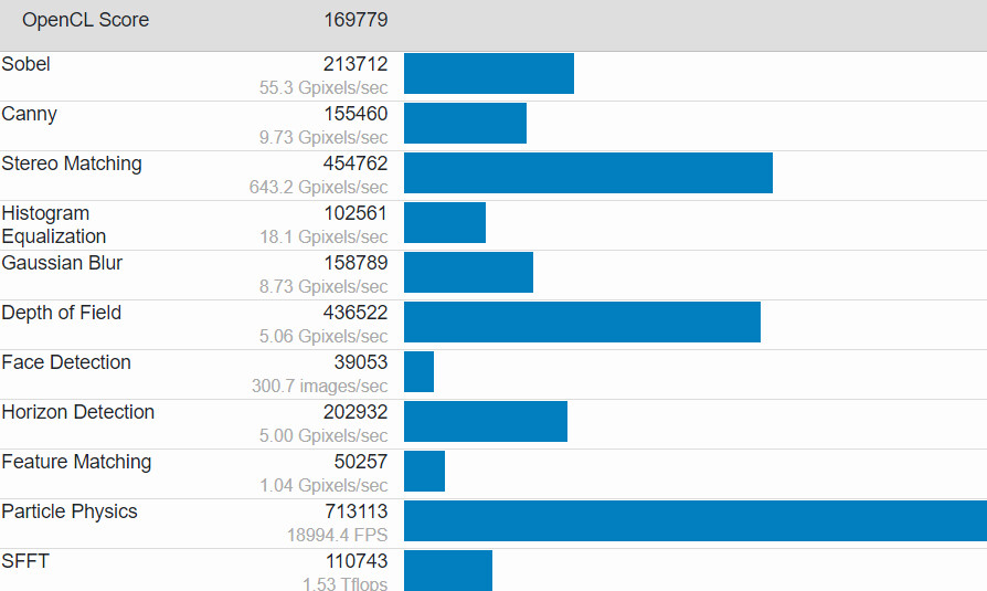
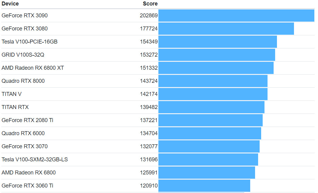
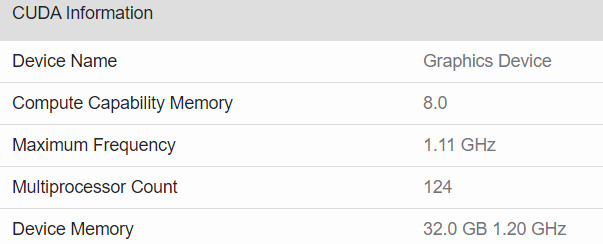
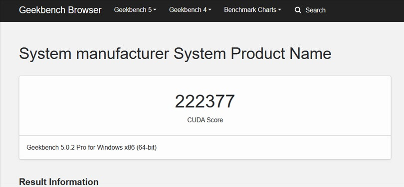
The NVIDIA MX550 has allegedly surfaced as part of a new Lenovo laptop in a Geekbench listing paired with an Intel Core i7-1260P 12 core, 16 thread processor. The card is described as a "Graphics Device" in the Geekbench listing however according to ITHome this is actually the upcoming MX550 entry-level mobile graphics card. The card is supposedly based on the Ampere GA107 GPU with 16 Compute Units and 128 CUDA cores paired with 2 GB of GDDR6 memory. The MX550 is the successor to the MX450 launched in August 2020 and should offer a roughly 15% performance increase according to the Geekbench OpenCL score. We have limited information on the availability of the card or the remainder of the MX500 series except that NVIDIA may officially announce them sometime early next year.

Chinese Innosilicon Fenghua No.1 Graphics Card Supports PCIe 4.0, HDMI 2.1, GDDR6X, & DirectX

Chinese company Innosilicon Technology has recently announced their Fenghua No.1 high-performance server graphics card. The card features a dual-fan cooling design with HDMI 2.1 and Embedded DisplayPort 1.4 video connectors. The card will utilize a PCIe 4.0 connector and features GDDR6X memory developed by Innosilicon Technology with potential speeds of 21 Gbps. We have seen announcements from Chinese companies with similar products in the past but this recent announcement is the first to include support for a variety of graphics APIs including DirectX. The press release from the company didn't specify the DirectX version supported but also noted that the card will support OpenGL, OpenGLES, OpenCL, and Vulkan which will enable VR, AR, and AI applications.

AMD Radeon PRO V620 GPU Delivers Powerful, Multi-Purpose Data Center Visual Performance for Today's Demanding Cloud Workloads

AMD announced the AMD Radeon PRO V620 GPU, built with the latest AMD RDNA 2 architecture which delivers high-performance GPU acceleration for today's demanding cloud workloads including immersive AAA game experiences, intensive 3D workloads and modern office productivity applications at scale in the cloud.

With its innovative GPU-partitioning capabilities, multi-stream hardware accelerated encoders and 32 GB GDDR6 memory, the AMD Radeon PRO V620 offers dedicated GPU resources that scale to multiple graphics users, helping ensure cost-effective graphics acceleration for a range of workloads. Built using the same GPU architecture that powers the latest generation game consoles and PC game experiences, the AMD Radeon PRO V620 GPU is also designed to develop and deliver immersive AAA game experiences.

Jingjia Micro JM9 GPU Series Targeting GTX 1080 Performance Tapes Out

The Chinese Electronics company Jingjia Micro have recently completed the tapeout of their JM9 GPU series almost 2 years after they first announced the lineup. The JM9 series will consist of two GPUs with the entry-level JM9231 targeting GTX 1050 performance while the higher-end JM9271 aims for the GTX 1080. The JM9231 is stated to feature a clock speed above 1.5 GHz, 8 GB of GDDR5 memory, and will provide 2 TFLOPS of performance within a 150 W TDP through a PCIe Gen3 x16 interface. The JM9271 increases the clock speed to above 1.8 GHz and is paired with 16 GB of HBM memory which should offer 8 TFLOPS of single-precision performance to rival the GTX 1080. The card manages to do this within a TDP package of 200 W and also includes PCIe Gen4 x16 support. The two cards both support HDMI 2.0 in addition to DisplayPort 1.3 for the JM9231 and DisplayPort 1.4 for the JM9271.

While the JM9271 may target GTX 1080 performance it only features OpenGL and OpenCL API support lacking DirectX or Vulkan compatibility greatly reducing its use for gaming. The cards were originally expected to be available in 2020 but after various delays they are now ready to enter production. These products are highly unlikely to make their way outside of the Chinese mainland and if they did we wouldn't expect them to have much impact on the global market.

Hackers Innovate Way to Store and Execute Malware from Video Memory to Evade Anti-Malware

Cybercriminals have innovated a way to store malware code inside GPU dedicated memory (video memory), and execute code directly from there. Execution from video memory may not be new, but they've mostly been confined to the academic space, and unrefined. This would be the first time a proof-of-concept of a working tool that injects executables to video memory, surfaced on a hacker forum.

The tool relies on OpenCL 2.0, and its developers claim to have successfully tested it on Intel Gen9, AMD RDNA, NVIDIA Kepler, and NVIDIA Turing graphics architectures (i.e. UHD 620, UHD 630, Radeon RX 5700, GeForce GTX 740M, and GTX 1650). What makes this ingenious is that the malware binary is stored entirely in GPU memory address-space and is executed by the GPU, rather than the CPUs. Conventional anti-malware software are only known to scan the system memory, disks, and network traffic for malware; but not video memory. Hopefully this will change.

Intel DG2 GPU with 256 Execution Units Offers GTX 1050 Performance

We have been receiving several leaks for Intel's upcoming DG2 GPUs with a 256 Execution Unit model recently appearing on Geekbench paired with a 14-core Alder Lake mobile CPU. The Alder Lake mobile processor featured an integrated Xe GPU with 96 Execution Units which were also benchmarked. The 256 Execution Unit graphics card tested is likely derived from the mid-range DG2-384 GPU. The 96 EU DG2 iGPU featured a maximum frequency of 1.2 GHz while the 256 EU variant increased that to 1.4 GHz. The DG2-256 scored an OpenCL score of 18,450 points in the Geekbench 5 benchmark which places it at GTX 1050 performance level. The DG2-96 integrated GPU scored 6,500 points which is comparable to a GTX 460. While these performance numbers are low it is important to keep in mind that these are just early results from a mid-range mobile offering and Intel is planning to release cards with 512 Execution Units which should compete with the RTX 3070 Ti and 6700 XT.

GPU Memory Latency Tested on AMD's RDNA 2 and NVIDIA's Ampere Architecture

Graphics cards have been developed over the years so that they feature multi-level cache hierarchies. These levels of cache have been engineered to fill in the gap between memory and compute, a growing problem that cripples the performance of GPUs in many applications. Different GPU vendors, like AMD and NVIDIA, have different sizes of register files, L1, and L2 caches, depending on the architecture. For example, the amount of L2 cache on NVIDIA's A100 GPU is 40 MB, which is seven times larger compared to the previous generation V100. That just shows how much new applications require bigger cache sizes, which is ever-increasing to satisfy the needs.

Today, we have an interesting report coming from Chips and Cheese. The website has decided to measure GPU memory latency of the latest generation of cards - AMD's RDNA 2 and NVIDIA's Ampere. By using simple pointer chasing tests in OpenCL, we get interesting results. RDNA 2 cache is fast and massive. Compared to Ampere, cache latency is much lower, while the VRAM latency is about the same. NVIDIA uses a two-level cache system consisting out of L1 and L2, which seems to be a rather slow solution. Data coming from Ampere's SM, which holds L1 cache, to the outside L2 is taking over 100 ns of latency.

Intel Alder Lake Processor Tested, Big Cores Ramp Up to 3 GHz

Intel "Alder Lake" is the first processor generation coming from the company to feature the hybrid big.LITTLE type core arrangement and we are wondering how the configurations look like and just how powerful the next-generation processors are going to be. Today, a Geekbench submission has appeared that gave us a little more information about one out of twelve Alder Lake-S configurations. This time, we are getting an 8-core, 16-threaded design with all big cores and no smaller cores present. Such design with no little cores in place is exclusive to the Alder Lake-S desktop platform, and will not come to the Alder Lake-P processors designed for mobile platforms.

Based on the socket LGA1700, the processor was spotted running all of its eight cores at 2.99 GHz frequency. Please note that this is only an engineering sample and the clock speeds of the final product should be higher. It was paired with the latest DDR5 memory and NVIDIA GeForce RTX 2080 GPU. The OpenCL score this CPU ran has shown that it has provided the GPU with more than enough performance. Typically, the RTX 2080 GPU scores about 106101 points in Geekbench OpenCL tests. Paired with the Alder Lake-S CPU, the GPU has managed to score as much as 108068 points, showing the power of the new generation of cores. While there is still a lot of mystery surrounding the Alder Lake-S series, we have come to know that the big cores used are supposed to be very powerful.

EIZO Releases Rugged XMC GPGPU Card for Media Applications

EIZO Rugged Solutions Inc., a provider of ruggedized graphics and video products, has released the Condor NVP2009AxX - an XMC graphics and GPGPU card that supports various combinations of analog and digital outputs.

The new high-performance graphics card based on the NVIDIA Quadro P2000 GPU (chip-down GP107) supports four field customizable video output combinations of DisplayPort++, 3G-SDI, CVBS (NTSC/PAL/SECAM), and VGA (STANAG 3350, RS-170, RS-343) to provide flexibility and simplify inventory management for high-end surveillance customers. With multiple I/O configurations, the card can support a range of video resolutions up to 4K and custom resolutions under VGA configurations. It can be factory configured to customer specifications and/or field programmed to support complex, multi-video needs after deployment.

NVIDIA GeForce RTX 3080 Mobile Maxes Out "GA104" Silicon

With the desktop GeForce RTX 3080 being based on the "big" GeForce Ampere silicon, the "GA102," we wondered how NVIDIA would go about designing the RTX 3080 Mobile. It turns out that the company will max out the smaller "GA104" silicon on which the desktop RTX 3070 and RTX 3060 Ti, are based. An unreleased ASUS ROG Zephyrus Duo (GX551QS) gaming notebook's Geekbench online database entry reveals the name-string and streaming multiprocessor (SM) count of the RTX 3080 Mobile.

The Geekbench online database entry lists out the OpenCL device (GPU) name-string as "GeForce RTX 3080 Laptop GPU," and OpenCL compute unit (SM) count as 48. This corresponds with the maximum SM count of the "GA104," which features 6,144 Ampere CUDA cores spread across 24 TPCs (48 SM), 48 2nd generation RT cores, 192 3rd generation Tensor cores, 192 TMUs, and 96 ROPs. The Geekbench entry also reveals the video memory amount as 16 GB, maxing out the 256-bit wide GDDR6 memory interface of the "GA104," likely using 16 Gbit memory chips.

AMD Radeon RX 6900 XT Graphics Card OpenCL Score Leaks

AMD has launched its RDNA 2 based graphics cards, codenamed Navi 21. These GPUs are set to compete with NVIDIA's Ampere offerings, with the lineup covering the Radeon RX 6800, RX 6800 XT, and RX 6900 XT graphics cards. Until now, we have had reviews of the former two, but not the Radeon RX 6900 XT. That is because the card is coming at a later date, specifically on December 8th, in just a few days. As a reminder, the Radeon RX 6900 XT GPU is a Navi 21 XTX model with 80 Compute Units that give a total of 5120 Stream Processors. The graphics card uses a 256-bit bus that connects the GPU with 128 MB of its Infinity Cache to 16 GB of GDDR6 memory. When it comes to frequencies, it has a base clock of 1825 MHz, with a boost speed of 2250 MHz.

Today, in a GeekBench 5 submission, we get to see the first benchmarks of AMD's top-end Radeon RX 6900 XT graphics card. Running an OpenCL test suite, the card was paired with AMD's Ryzen 9 5950X 16C/32T CPU. The card managed to pass the OpenCL test benchmarks with a score of 169779 points. That makes the card 12% faster than RX 6800 XT GPU, but still slower than the competing NVIDIA GeForce RTX 3080 GPU, which scores 177724 points. However, we need to wait for a few more benchmarks to appear to jump to any conclusions, including the TechPowerUp review, which is expected to arrive once NDA lifts. Below, you can compare the score to other GPUs in the GeekBench 5 OpenCL database.

AMD Radeon RX 6800 and RX 6800 XT GPU OpenCL Performance Leaks

AMD has just recently announced its next-generation Radeon RX 6000 series GPU based on the new RDNA 2 architecture. The architecture is set to compete with NVIDIA Ampere architecture and highest offerings of the competing company. Today, thanks to the well-known leaker TUM_APISAK, we have some Geekbench OpenCL scores. It appears that some user has gotten access to the system with the Radeon RX 6800 and RX 6800 XT GPUs, running Cinebench 4.4 OpenCL tests. In the tests, the system ran on the Intel platform with Core i9-10900K CPU with 16 GB DDR4 RAM running at 3600 MHz. The motherboard used was ASUS top-end ROG Maximus XII Extreme Z490 board.

When it comes to results, the system with RX 6800 GPU scored anywhere from 347137 points to 336367 points in three test runs. For comparison, NVIDIA GeForce RTX 3070 scores about 361042 points, showcasing that the Radeon card is not faster in any of the runs. When it comes to the higher-end Radeon RX 6800 XT GPU, it scored 407387 and 413121 points in two test runs. Comparing that to GeForce RTX 3080 GPU that scores 470743 points, the card is slower compared to the competition. There has been a Ryzen 9 5950X test setup that boosted the performance of Radeon RX 6800 XT card by quite a lot, making it reach 456837 points, making a huge leap over the Intel-based system thanks to the Smart Access Memory (SAM) technology that all-AMD system provides.

Intel Xe-HP "NEO Graphics" GPU with 512 EUs Spotted

Intel is preparing to flood the market with its Xe GPU lineup, covering the entire vector from low-end to high-end consumer graphics cards. Just a few days ago, the company has announced its Iris Xe MAX GPU, the first discrete GPU from Intel, aimed at 1080p gamer and content creators. However, that seems to be only the beginning of Intel's GPU plan and just a small piece of the entire lineup. Next year, the company is expected to launch two GPU families - Xe-HP and Xe-HPG. With the former being a data-centric GPU codenamed Arctic Sound, and the latter being a gaming-oriented GPU called DG2. Today, thanks to the GeekBench listing, we have some information on the Xe-HP GPU.

Being listed with 512 EUs (Execution Units), translating into 4096 shading units, the GPU is reportedly a Xe-HP variant codenamed "NEO Graphics". This is not the first time that the NEO graphics has been mentioned. Intel has called a processor Neo graphics before, on its Architecture day when the company was demonstrating the FP32 performance. The new GeekBench leak shows the GPU running at 1.15 GHz clock speed, where at the Architecture day the same GPU ran at 1.3 GHz frequency, indicating that this is only an engineering sample. The GPU ran the GeekBench'es OpenCL test and scored very low 25,475 points. Compared to NVIDIA's GeForce RTX 3070 GPU that scored 140,484, the Intel GPU is at least four times slower. That is possibly due to the non-optimization of the benchmark, which could greatly improve in the future. In the first picture below, this Xe-HP GPU would represent the single-tile design.

Khronos Group Releases SYCL 2020 Provisional Specification

Today, The Khronos Group, an open consortium of industry-leading companies creating graphics and compute interoperability standards, announces the ratification and public release of the SYCL 2020 Provisional Specification. SYCL is a standard C++ based heterogeneous parallel programming framework for accelerating High Performance Computing (HPC), machine learning, embedded computing, and compute-intensive desktop applications on a wide range of processor architectures, including CPUs, GPUs, FPGAs, and AI processors.The SYCL 2020 Provisional Specification is publicly available today to enable feedback from developers and implementers before the eventual specification finalization and release of the SYCL 2020 Adopters Program, which will enable implementers to be officially conformant—tentatively expected by the end of the year.

A royalty-free open standard, SYCL 2020 enables significant programmer productivity through an expressive domain-specific language, compact code, and simplified common patterns, such as Class Template Argument Deduction and Deduction Guides, all while preserving significant backwards compatibility with previous versions. SYCL 2020 is based on C++17 and includes new programming abstractions, such as unified shared memory, reductions, group algorithms, and sub-groups to enable high-performance applications across diverse hardware architectures.

AMD EPYC Scores New Supercomputing and High-Performance Cloud Computing System Wins

AMD today announced multiple new high-performance computing wins for AMD EPYC processors, including that the seventh fastest supercomputer in the world and four of the 50 highest-performance systems on the bi-annual TOP500 list are now powered by AMD. Momentum for AMD EPYC processors in advanced science and health research continues to grow with new installations at Indiana University, Purdue University and CERN as well as high-performance computing (HPC) cloud instances from Amazon Web Services, Google, and Oracle Cloud.

"The leading HPC institutions are increasingly leveraging the power of 2nd Gen AMD EPYC processors to enable cutting-edge research that addresses the world's greatest challenges," said Forrest Norrod, senior vice president and general manager, data center and embedded systems group, AMD. "Our AMD EPYC CPUs, Radeon Instinct accelerators and open software programming environment are helping to advance the industry towards exascale-class computing, and we are proud to strengthen the global HPC ecosystem through our support of the top supercomputing clusters and cloud computing environments."

DirectX Coming to Linux...Sort of

Microsoft is preparing to add the DirectX API support to WSL (Windows Subsystem for Linux). The latest Windows Subsystem for Linux 2 will virtualize DirectX to Linux applications running on top of it. WSL is a translation layer for Linux apps to run on top of Windows. Unlike Wine, which attempts to translate Direct3D commands to OpenGL, what Microsoft is proposing is a real DirectX interface for apps in WSL, which can essentially talk to hardware (the host's kernel-mode GPU driver) directly.

To this effect, Microsoft introduced the Linux-edition of DXGkrnl, a new kernel-mode driver for Linux that talks to the DXGkrnl driver of the Windows host. With this, Microsoft is promising to expose the full Direct3D 12, DxCore, and DirectML. It will also serve as a conduit for third party APIs, such as OpenGL, OpenCL, Vulkan, and CUDA. Microsoft expects to release this feature-packed WSL out with WDDM 2.9 (so a future version of Windows 10).

Intel Gen12 Xe DG1 OpenCL Performance Geekbenched

Intel's ambitious Xe graphics architecture is expected to make its first commercial debut as an iGPU that's part of the company's 11th gen Core "Tiger Lake" mobile processors, but it already received a non-commercial distribution as a discrete GPU called the DG1, with Intel shipping it to its independent software vendor ecosystem partners to begin exploratory work on Xe. One such ISV paired the card with a Core i7-8700 processor, and put it through Geekbench. While the Geekbench device identification doesn't mention "DG1," we lean toward the possibility looking at its 96 EU configuration, and 1.50 GHz clock speed, and 3 GB memory.

The Geekbench run only covers OpenCL performance of the selected device: "Intel(R) Gen12 Desktop Graphics Controller." The total score is 55373 points, with 3.53 Gpixels/s in "Sorbel," 1.30 Gpixels/sec in Histogram Equalization, 16 GFLOPs in SFFT, 1.62 GPixels/s in Gaussian Blur, 4.51 Msubwindows/s in Face Detection, 2.88 Gpixels/s in RAW, 327.4 Mpixels/s in DoF, and 13656 FPS in Particle Physics. These scores roughly match the 11 CU Radeon Vega iGPU found in AMD "Picasso" Ryzen 5 3400G processors.

AMD Announces Radeon Pro VII Graphics Card, Brings Back Multi-GPU Bridge

AMD today announced its Radeon Pro VII professional graphics card targeting 3D artists, engineering professionals, broadcast media professionals, and HPC researchers. The card is based on AMD's "Vega 20" multi-chip module that incorporates a 7 nm (TSMC N7) GPU die, along with a 4096-bit wide HBM2 memory interface, and four memory stacks adding up to 16 GB of video memory. The GPU die is configured with 3,840 stream processors across 60 compute units, 240 TMUs, and 64 ROPs. The card is built in a workstation-optimized add-on card form-factor (rear-facing power connectors and lateral-blower cooling solution).

What separates the Radeon Pro VII from last year's Radeon VII is full double precision floating point support, which is 1:2 FP32 throughput compared to the Radeon VII, which is locked to 1:4 FP32. Specifically, the Radeon Pro VII offers 6.55 TFLOPs double-precision floating point performance (vs. 3.36 TFLOPs on the Radeon VII). Another major difference is the physical Infinity Fabric bridge interface, which lets you pair up to two of these cards in a multi-GPU setup to double the memory capacity, to 32 GB. Each GPU has two Infinity Fabric links, running at 1333 MHz, with a per-direction bandwidth of 42 GB/s. This brings the total bidirectional bandwidth to a whopping 168 GB/s—more than twice the PCIe 4.0 x16 limit of 64 GB/s.

Khronos Group Releases OpenCL 3.0

Today, The Khronos Group, an open consortium of industry-leading companies creating advanced interoperability standards, publicly releases the OpenCL 3.0 Provisional Specifications. OpenCL 3.0 realigns the OpenCL roadmap to enable developer-requested functionality to be broadly deployed by hardware vendors, and it significantly increases deployment flexibility by empowering conformant OpenCL implementations to focus on functionality relevant to their target markets. OpenCL 3.0 also integrates subgroup functionality into the core specification, ships with a new OpenCL C 3.0 language specification, uses a new unified specification format, and introduces extensions for asynchronous data copies to enable a new class of embedded processors. The provisional OpenCL 3.0 specifications enable the developer community to provide feedback on GitHub before the specifications and conformance tests are finalized.
OpenCL

Three Unknown NVIDIA GPUs GeekBench Compute Score Leaked, Possibly Ampere?

(Update, March 4th: Another NVIDIA graphics card has been discovered in the Geekbench database, this one featuring a total of 124 CUs. This could amount to some 7,936 CUDA cores, should NVIDIA keep the same 64 CUDA cores per CU - though this has changed in the past, as when NVIDIA halved the number of CUDA cores per CU from Pascal to Turing. The 124 CU graphics card is clocked at 1.1 GHz and features 32 GB of HBM2e, delivering a score of 222,377 points in the Geekbench benchmark. We again stress that these can be just engineering samples, with conservative clocks, and that final performance could be even higher).

NVIDIA is expected to launch its next-generation Ampere lineup of GPUs during the GPU Technology Conference (GTC) event happening from March 22nd to March 26th. Just a few weeks before the release of these new GPUs, a Geekbench 5 compute score measuring OpenCL performance of the unknown GPUs, which we assume are a part of the Ampere lineup, has appeared. Thanks to the twitter user "_rogame" (@_rogame) who obtained a Geekbench database entry, we have some information about the CUDA core configuration, memory, and performance of the upcoming cards.
NVIDIA Ampere CUDA Information NVIDIA Ampere Geekbench

Imagination launches IMG A-Series Graphics Architecture: "The GPU of Everything"

Imagination Technologies announces the tenth generation of its PowerVR graphics architecture, the IMG A-Series. The fastest GPU IP ever released, IMG A-Series evolves the PowerVR GPU architecture to fulfil the graphics and compute needs of the full spectrum of next-generation devices. Designed to be "The GPU of Everything" IMG A-Series is the ultimate solution for multiple markets, from automotive, AIoT, and computing through to DTV/STB/OTT, mobile and server.

The IMG A-Series' multi-dimensional approach to performance scalability ranges from 1 pixel per clock (PPC) parts for the entry-level market right up to 2 TFLOP cores for performance devices, and beyond that to multi-core solutions for cloud applications. Dr. Ron Black, CEO, Imagination Technologies, says: "IMG A-Series is our most important GPU launch since we delivered the first mobile PowerVR GPU 15 years ago and the best GPU IP for mobile ever made. It offers the best performance over sustained time periods and at low power budgets across all markets. It really is the GPU of everything."

AMD Radeon "Navi" OpenCL Bug Makes it Unfit for SETI@Home

A bug with the Radeon RX 5700-series "Navi" OpenCL compute API ICD (installable client driver) is causing the GPUs to crunch incorrect results for distributed compute project SETI@Home. Since there are "many" Navi GPUs crunching the project cross-validating each others' incorrect results, the large volume of incorrect results are able to beat the platform's algorithm and passing statistical validation, "polluting" the SETI@Home database. Some volunteers at the SETI@Home forums, where the the issue is being discussed, advocate banning or limiting results from contributors using these GPUs, until AMD comes out with a fix for its OpenCL driver. SETI@Home is a distributed computing project run by SETI (Search for Extraterrestrial Intelligence), tapping into volunteers' compute power to make sense of radio waves from space.

7nm Intel Xe GPUs Codenamed "Ponte Vecchio"

Intel's first Xe GPU built on the company's 7 nm silicon fabrication process will be codenamed "Ponte Vecchio," according to a VideoCardz report. These are not gaming GPUs, but rather compute accelerators designed for exascale computing, which leverage the company's CXL (Compute Express Link) interconnect that has bandwidth comparable to PCIe gen 4.0, but with scalability features slated to come out with future generations of PCIe. Intel is preparing its first enterprise compute platform featuring these accelerators codenamed "Project Aurora," in which the company will exert end-to-end control over not just the hardware stack, but also the software.

"Project Aurora" combines up to six "Ponte Vecchio" Xe accelerators with up to two Xeon multi-core processors based on the 7 nm "Sapphire Rapids" microarchitecture, and OneAPI, a unifying API that lets a single kind of machine code address both the CPU and GPU. With Intel owning the x86 machine architecture, it's likely that Xe GPUs will feature, among other things, the ability to process x86 instructions. The API will be able to push scalar workloads to the CPU, and and the GPU's scalar units, and vector workloads to the GPU's vector-optimized SIMD units. Intel's main pitch to the compute market could be significantly lowered software costs from API and machine-code unification between the CPU and GPU.
Image Courtesy: Jan Drewes

TechPowerUp Releases GPU-Z v2.21.0

TechPowerUp GPU-Z is a handy graphics subsystem information, diagnostic, and monitoring utility no enthusiast can leave home without, and today we bring you its latest version. The new TechPowerUp GPU-Z v2.21.0 adds support for NVIDIA Quadro P500. More importantly, it fixes sensor data readouts being broken for the Radeon VII with Radeon Software 19.5.1 (or later) installed. A broken GPU load sensor for AMD "Raven Ridge" APUs has also been fixed. Lastly, OpenCL support detection has been added for Radeon VII and other graphics cards based on the "Vega 20" MCM. Grab it from the link below.
DOWNLOAD: TechPowerUp GPU-Z

The change-log follows.

It Can't Run Crysis: Radeon Instinct MI60 Only Supports Linux

AMD recently announced the Radeon Instinct MI60, a GPU-based data-center compute processor with hardware virtualization features. It takes the crown for "the world's first 7 nm GPU." The company also put out specifications of the "Vega 20" GPU it's based on: 4,096 stream processors, 4096-bit HBM2 memory interface, 1800 MHz engine clock-speed, 1 TB/s memory bandwidth, 7.4 TFLOP/s peak double-precision (FP64) performance, and the works. Here's the kicker: the company isn't launching this accelerator with Windows support. At launch, AMD is only releasing x86-64 Linux drivers, with API support for OpenGL 4.6, Vulkan 1.0, and OpenCL 2.0, along with AMD's ROCm open ecosystem. The lack of display connector already disqualifies this card for most workstation applications, but with the lack of Windows support, it is also the most expensive graphics card that "can't run Crysis." AMD could release Radeon Pro branded graphics cards based on "Vega 20," which will ship with Windows and MacOS drivers.
Return to Keyword Browsing
Jul 5th, 2025 20:58 CDT change timezone

New Forum Posts

Popular Reviews

TPU on YouTube

Controversial News Posts