TSMC Plans CoPoS and SoIC Advanced Packaging for Arizona Fab
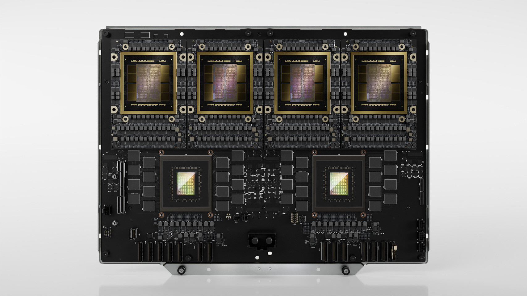
TSMC plans to expand its Arizona facility with advanced packaging by constructing two dedicated buildings near to its Fab 21 complex. The first, Advanced Packaging Facility 1 (AP1), is slated to break ground in 2028 alongside Phase 3 of Fab 21, which will eventually produce chips on the N2 (2 nm) node and potentially the A16 process. A second structure, AP2, will follow in tandem with later expansions (Phases 4 and 5), though exact dates remain unconfirmed. Both sites will focus on System‑on‑Integrated‑Chips (SoIC) and the emerging Chip‑on‑Panel‑on‑Substrate (CoPoS) technology. SoIC uses through‑silicon vias to stack cache or memory dies directly beneath compute cores, a technique already proven in AMD's Ryzen X3D processors. CoPoS, by contrast, replaces traditional circular wafers with rectangular panels measuring approximately 310x310 mm.
This shift multiplies the usable substrate area by more than five times, enabling the denser integration of high-bandwidth memory stacks, I/O chiplets, and multiple compute tiles while driving down per-unit costs. Behind the scenes, TSMC will kick off a CoPoS pilot line as early as 2026, aiming to complete partner validation by late 2027. This pilot run is designed to address manufacturing challenges and secure design wins with major customers, including NVIDIA, AMD, and Apple, ensuring that US‑assembled packages meet the same performance and reliability standards as those in Taiwan. Mass production at AP1 is not expected to ramp up until late 2029 or early 2030, aligning with TSMC's two-year lead-time practice: new node and packaging innovations debut on the home island before being transplanted abroad.

This shift multiplies the usable substrate area by more than five times, enabling the denser integration of high-bandwidth memory stacks, I/O chiplets, and multiple compute tiles while driving down per-unit costs. Behind the scenes, TSMC will kick off a CoPoS pilot line as early as 2026, aiming to complete partner validation by late 2027. This pilot run is designed to address manufacturing challenges and secure design wins with major customers, including NVIDIA, AMD, and Apple, ensuring that US‑assembled packages meet the same performance and reliability standards as those in Taiwan. Mass production at AP1 is not expected to ramp up until late 2029 or early 2030, aligning with TSMC's two-year lead-time practice: new node and packaging innovations debut on the home island before being transplanted abroad.