News Posts matching #chiplets

Return to Keyword Browsing

Arteris Accelerates AI-Driven Silicon Innovation with Expanded Multi-Die Solution

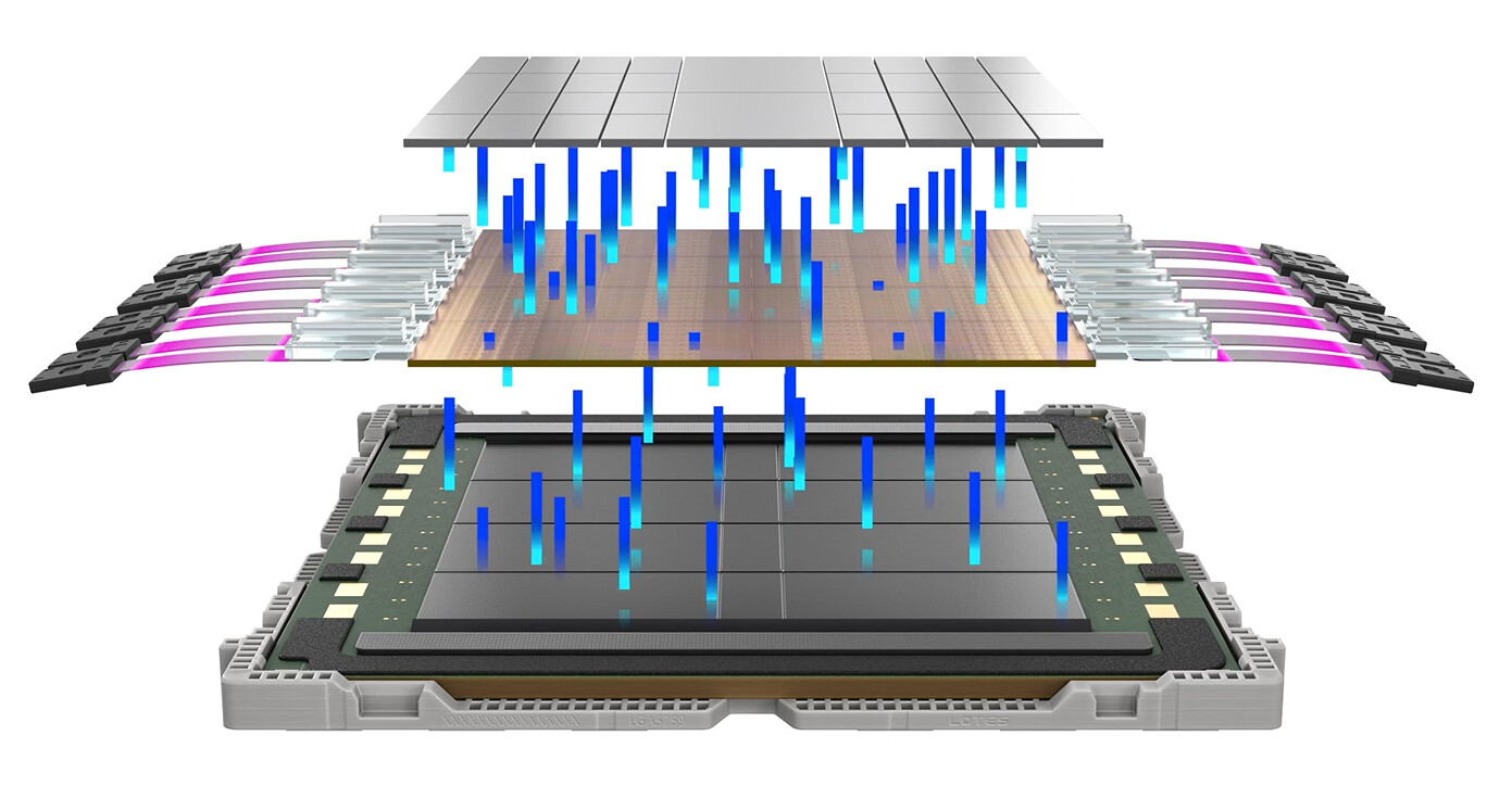
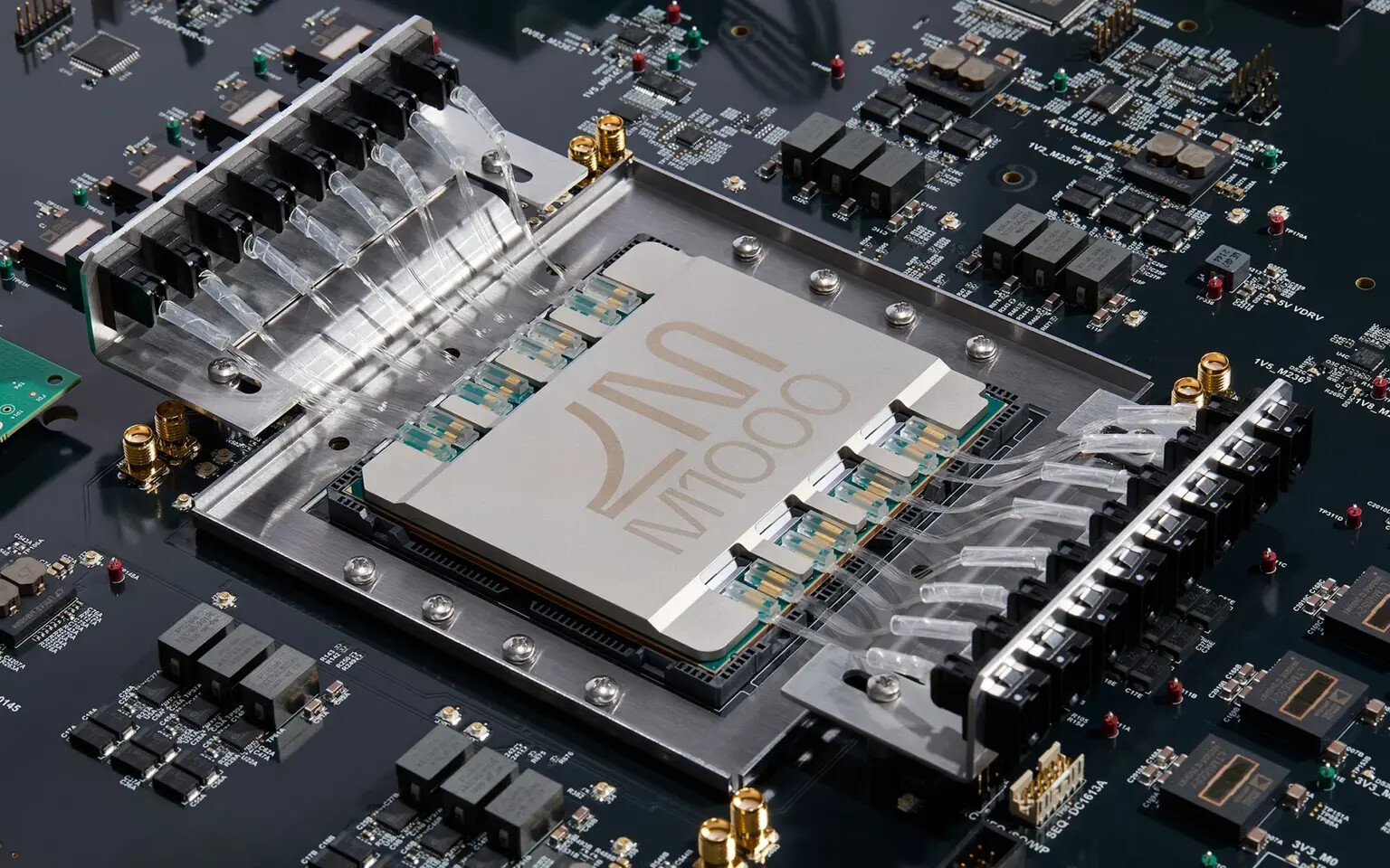
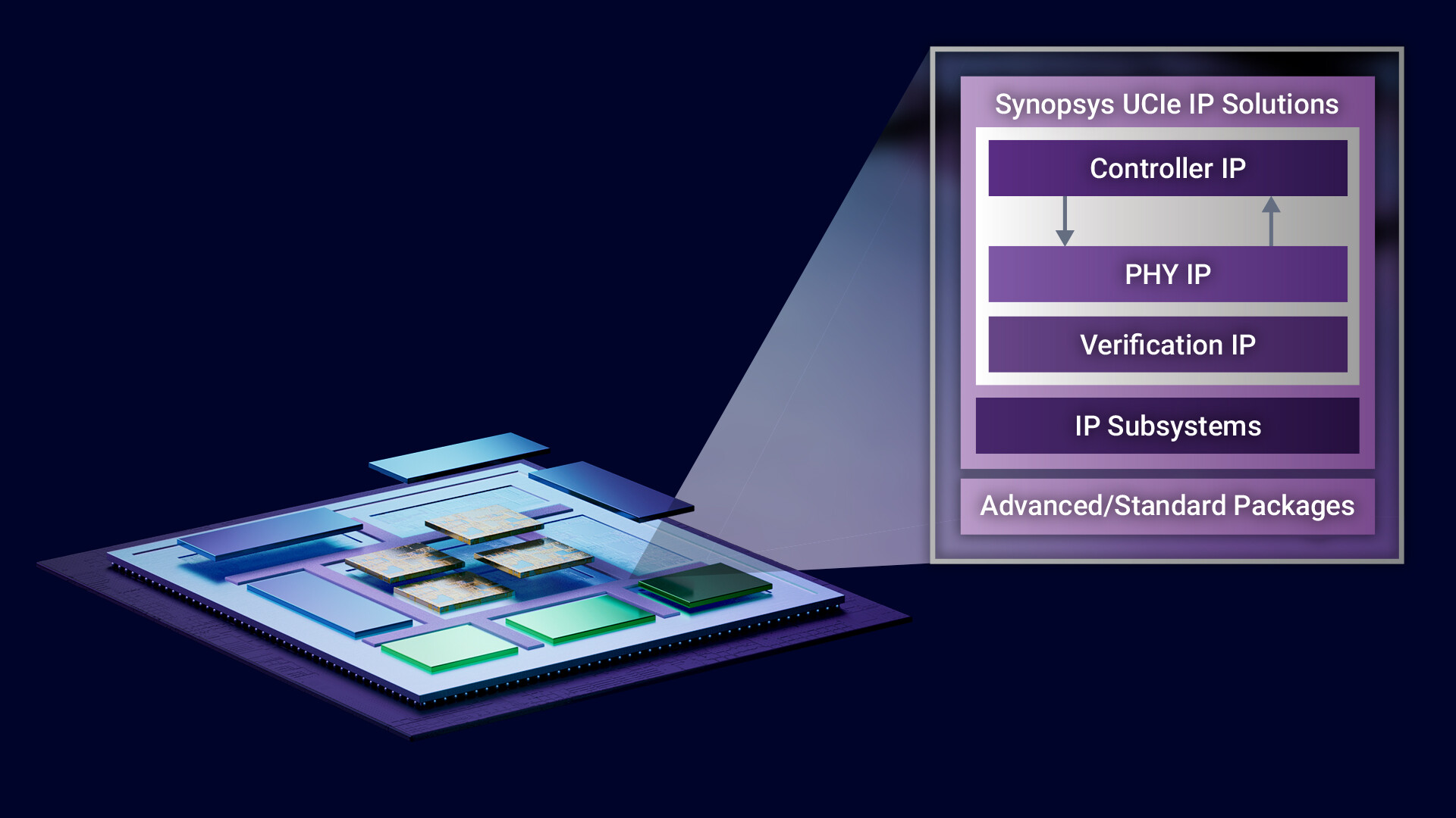
In a market reshaped by the compute demands of AI, Arteris, Inc. (Nasdaq: AIP), a leading provider of system IP for accelerating semiconductor creation, today announced an expansion of its multi-die solution, delivering a foundational technology for rapid chiplet-based innovation. "In the chiplet era, the need for computational power increasingly exceeds what is available by traditional monolithic die designs," said K. Charles Janac, president and CEO of Arteris. "Arteris is leading the transition into the chiplet era with standards-based, automated and silicon-proven solutions that enable seamless integration across IP cores, chiplets, and SoCs."

Moore's Law, predicting the doubling of transistor count on a chip every two years, is slowing down. As the semiconductor industry accelerates efforts to increase performance and efficiency, especially driven by AI workloads, architectural innovation through multi-die systems has become critical. Arteris' expanded multi-die solution addresses this shift with a suite of enhanced technologies that are purpose-built for scalable and faster time-to-silicon, high-performance computing, and automotive-grade mission-critical designs.

Taiwan Adds Huawei and SMIC to Export Control List, TSMC First to Comply

On June 10, Taiwan's Ministry of Economic Affairs expanded its list of strategic export-controlled customers to include Huawei and Semiconductor Manufacturing International Corporation (SMIC). The ministry announced that this decision followed a review meeting focused on preventing the proliferation of arms and other national security concerns. Moving forward, any Taiwanese exporter must obtain formal government approval before shipping semiconductors, lithography machines, or related equipment to Huawei or SMIC. TSMC immediately confirmed its full compliance. Company representatives reminded stakeholders that no orders have been fulfilled for Huawei since September 2020 and pledged to enhance internal verification procedures to block any unauthorized transactions. These steps build on one‑billion‑dollar penalty, imposed after investigators determined that two million advanced AI chiplets had been supplied for Huawei's Ascend 910B accelerator without proper clearance.

For Huawei and SMIC, this latest measure compounds the challenges created by existing US export controls, which prohibit both companies from sourcing many US-origin technologies and designs. The two Chinese giants will accelerate efforts to develop domestic alternatives, yet true semiconductor independence remains a distant goal. Designing and building reliable extreme ultraviolet lithography systems demands years of specialized research and highly precise manufacturing capabilities. Scaling production without foreign expertise could introduce costly delays. In response, Chinese research institutes report that the country's first homegrown EUV lithography machines are slated to enter trial production in the third quarter of 2025. Meanwhile, state‑backed partners are racing to develop advanced packaging tools to rival those offered by ASML. Despite these initiatives, experts warn that catching up with global leaders will require substantial time and continued investment.

TSMC Prepares "CoPoS": Next-Gen 310 × 310 mm Packages

As demand for ever-growing AI compute power continues to rise and manufacturing advanced nodes becomes more difficult, packaging is undergoing its golden era of development. Today's advanced accelerators often rely on TSMC's CoWoS modules, which are built on wafer cuts measuring no more than 120 × 150 mm in size. In response to the need for more space, TSMC has unveiled plans for CoPoS, or "Chips on Panel on Substrate," which could expand substrate dimensions to 310 × 310 mm and beyond. By shifting from round wafers to rectangular panels, CoPoS offers more than five times the usable area. This extra surface makes it possible to integrate additional high-bandwidth memory stacks, multiple I/O chiplets and compute dies in a single package. It also brings panel-level packaging (PLP) to the fore. Unlike wafer-level packaging (WLP), PLP assembles components on large, rectangular panels, delivering higher throughput and lower cost per unit. Systems with PLP will be actually viable for production runs and allow faster iterations over WLP.

TSMC will establish a CoPoS pilot line in 2026 at its Visionchip subsidiary. In 2027, the pilot facility will focus on refining the process, to meet partner requirements by the end of the year. Mass production is projected to begin between the end of 2028 and early 2029 at TSMC's Chiayi AP7 campus. That site, chosen for its modern infrastructure and ample space, is also slated to host production of multi-chip modules and System-on-Wafer technologies. NVIDIA is expected to be the launch partner for CoPoS. The company plans to leverage the larger panel area to accommodate up to 12 HBM4 chips alongside several GPU chiplets, offering significant performance gains for AI workloads. At the same time, AMD and Broadcom will continue using TSMC's CoWoS-L and CoWoS-R variants for their high-end products. Beyond simply increasing size, CoPoS and PLP may work in tandem with other emerging advances, such as glass substrates and silicon photonics. If development proceeds as planned, the first CoPoS-enabled devices could reach the market by late 2029.

Siemens and Intel Foundry Collaborates on Integrated Circuits and Advanced Packaging Solutions for 2D and 3D IC

Siemens Digital Industries Software today announced that its continued collaboration with Intel Foundry has resulted in multiple product certifications, updated foundry reference flows, and additional technology enablement leveraging the foundry's leading-edge technologies for next-generation integrated circuits (IC) and advanced packaging. Siemens is a founding partner of the Intel Foundry Accelerator Chiplet Alliance - enabling a new and compelling solution for 3D IC and chiplet offerings to a breadth of semiconductor market verticals.

Intel 18A Certification Achievements
Siemens' industry-leading Calibre nmPlatform tool is now certified for the latest Intel 18A production Process Design Kit (PDK). Intel 18A represents a significant technological leap forward, featuring innovative RibbonFET Gate-all-around transistors and the industry's first PowerVia backside power delivery. This Calibre certification allows mutual customers to continue leveraging the Calibre nmPlatform tool as their industry-standard sign-off solution with Intel Foundry's most advanced manufacturing process, accelerating time-to-market for next-generation chip designs.

Ansys Thermal and Multiphysics Solutions Certified for Intel 18A Process and 3D-IC Designs

Ansys today announced thermal and multiphysics signoff tool certifications for designs manufactured with Intel 18A process technology. These certifications help ensure functionality and reliability of advanced semiconductor systems for the most demanding applications—including AI chips, graphic processing units (GPUs), and high-performance computing (HPC) products. Intel Foundry and Ansys have also enabled a comprehensive multiphysics signoff analysis flow for Intel Foundry's EMIB technology used for creating multi-die 3D integrated circuit (3D-IC) systems.

Recognized as industry-leading solutions, RedHawk-SC and Totem deliver speed, accuracy, and capacity to analyze the power integrity and reliability of Intel 18A RibbonFET Gate-all-around (GAA) transistors with PowerVia backside power delivery. For scalable electromagnetic analysis, Ansys is introducing HFSS-IC Pro, a new addition to the HFSS-IC product family. HFSS-IC Pro is certified for modeling on-chip electromagnetic integrity in radio frequency chips, Wi-Fi, 5G/6G, and other telecommunication applications made with the Intel 18A process node.

Avicena Works with TSMC to Enable PD Arrays for LightBundle MicroLED-Based Interconnects

Avicena, headquartered in Sunnyvale, CA, announced today that the company will work with TSMC to optimize photodetector (PD) arrays for Avicena's revolutionary LightBundle microLED-based interconnects. LightBundle supports > 1Tbps/mm shoreline density and extends ultra-high density die-to-die (D2D) connections to > 10 meters at class-leading sub-pJ/bit energy efficiency. This will enable AI scale-up networks to support large clusters of GPUs across multiple racks, eliminating reach limitations of current copper interconnects while drastically reducing power consumption.

Increasingly sophisticated AI models are driving an unprecedented surge in demand for compute and memory performance, requiring interconnects with higher density, lower power, and longer reach for both processor-to-processor (P2P) and processor-to-memory (P2M) connectivity.

TSMC Faces $1 Billion Fine from US Government Over Shipments to Huawei

TSMC is confronting a potential $1 billion-plus penalty from the US Commerce Department after inadvertently fabricating compute chiplets later integrated into Huawei's Ascend 910 AI processor. The fine, potentially reaching twice the value of unauthorized shipments, reflects the scale of components that circumvented export controls limiting Chinese access to advanced semiconductor technology. The regulatory breach originated in late 2023 when TSMC processed orders from Sophgo, a design partner of crypto-mining firm Bitmain. These chiplets, which are manufactured on advanced process nodes and contain tens of billions of transistors, were identified in TechInsights teardown analysis of Huawei Ascend 910 AI accelerator, revealing a supply chain vulnerability where TSMC lacked visibility into the components' end-use.

Upon discovery of the diversion, TSMC immediately halted Sophgo shipments and engaged in discussions with Commerce Department officials. By January, Sophgo had been added to the Entity List, limiting its access to US semiconductor technology. A Center for Strategic and International Studies report revealed that Huawei obtained approximately two million Ascend 910B logic dies through shell companies that misled TSMC. Huawei's preference for TSMC-made dies was due to manufacturing challenges in domestic chip production. This incident has forced TSMC to strengthen its customer vetting protocols, including terminating its relationship with Singapore-based PowerAIR following internal compliance reviews. The enforcement process typically begins with a proposed charging letter detailing violations and penalty calculations, followed by a 30-day response period. As Washington tightens restrictions on AI processor exports to Chinese entities, semiconductor manufacturers are under increased pressure to implement rigorous controls throughout multinational supply chains.

Lightmatter Unveils Passage M1000 Photonic Superchip

Lightmatter, the leader in photonic supercomputing, today announced Passage M1000, a groundbreaking 3D Photonic Superchip designed for next-generation XPUs and switches. The Passage M1000 enables a record-breaking 114 Tbps total optical bandwidth for the most demanding AI infrastructure applications. At more than 4,000 square millimeters, the M1000 reference platform is a multi-reticle active photonic interposer that enables the world's largest die complexes in a 3D package, providing connectivity to thousands of GPUs in a single domain.

In existing chip designs, interconnects for processors, memory, and I/O chiplets are bandwidth limited because electrical input/output (I/O) connections are restricted to the edges of these chips. The Passage M1000 overcomes this limitation by unleashing electro-optical I/O virtually anywhere on its surface for the die complex stacked on top. Pervasive interposer connectivity is enabled by an extensive and reconfigurable waveguide network that carries high-bandwidth WDM optical signals throughout the M1000. With fully integrated fiber attachment supporting an unprecedented 256 fibers, the M1000 delivers an order of magnitude higher bandwidth in a smaller package size compared to conventional Co-Packaged Optics (CPO) and similar offerings.

Sarcina Technology Launches AI Chiplet Platform Enabling Systems Up to 100x100 mm in a Single Package

Sarcina Technology, a global semiconductor packaging specialist, is excited to announce the launch of its innovative AI platform to enable advanced AI packaging solutions that can be tailored to meet specific customer requirements. Leveraging ASE's FOCoS-CL (Fan-Out Chip-on-Substrate-Chip Last) assembly technology, this platform includes an interposer which supports chiplets using UCIe-A for die-to-die interconnects, allowing for the delivery of cost-effective, customizable, cutting-edge solutions.

Sarcina Technology is on a mission to push the boundaries of AI computing system development by providing a unique platform that enables efficient, scalable, configurable and cost-effective semiconductor packaging solutions for AI applications. As AI workloads continue to evolve, there is a need for increasingly sophisticated packaging solutions capable of supporting higher computational demands. Sarcina's novel interposer packaging technology integrates leading memory solutions with high-efficiency interconnects. Whether prioritizing cost, performance or power-efficiency, Sarcina's new AI platform can deliver.

Marvell Demonstrates Industry's Leading 2nm Silicon for Accelerated Infrastructure

Marvell Technology, Inc., a leader in data infrastructure semiconductor solutions, has demonstrated its first 2 nm silicon IP for next-generation AI and cloud infrastructure. Produced on TSMC's 2 nm process, the working silicon is part of the Marvell platform for developing custom XPUs, switches and other technology to help cloud service providers elevate the performance, efficiency, and economic potential of their worldwide operations.

Given a projected 45% TAM growth annually, custom silicon is expected to account for approximately 25% of the market for accelerated compute by 20281.

Baya Systems and Semidynamics Collaborate to Accelerate RISC-V System-on-Chip Development

Baya Systems, a leader in system IP technology that empowers the acceleration of intelligent compute, and Semidynamics, a provider of fully customizable high-bandwidth and high-performance RISC-V processor IP, today announced a collaboration to boost innovation in development of hyper-efficient, next-generation platforms for artificial intelligence (AI), machine learning (ML) and high-performance computing (HPC) applications.

The collaboration integrates Semidynamics' family of 64-bit RISC-V processor IP cores, known for their exceptional memory bandwidth and configurability, with Baya Systems' innovative WeaveIP Network on Chip (NoC) system IP. WeaveIP is engineered for ultra-efficient, high-bandwidth, and low-latency data transport, crucial for the demands of modern workloads. Complementing this is Baya Systems' software-driven WeaverPro platform, which enables rapid system-level optimization, ensuring that key performance indicators (KPIs) are met based on real-world workloads while providing unparalleled design flexibility for future advancements.

APECS Chiplet Pilot Line Starts Operation in the Framework of the EU Chips Act

The pilot line for "Advanced Packaging and Heterogeneous Integration for Electronic Components and Systems" (APECS) marks a major leap forward in strengthening Europe's semiconductor manufacturing capabilities and chiplet innovation as part of the EU Chips Act. By providing large industry players, SMEs, and start-ups with a facilitated access to cutting-edge technology, the APECS pilot line will establish a strong foundation for resilient and robust European semiconductor supply chains. Within APECS, the institutes collaborating in the Research Fab Microelectronics Germany (FMD) will work closely with European partners, to make a significant contribution to the European Union's goals of increasing technological resilience, strengthening cross-border collaboration and enhancing its global competitiveness in semiconductor technologies. APECS is co-funded by the Chips Joint Undertaking and national funding authorities of Austria, Belgium, Finland, France, Germany, Greece, Portugal, Spain, through the "Chips for Europe" initiative. The overall funding for APECS amounts to €730 million over 4.5 years.

Europe is home to a vibrant ecosystem of (hidden) champions, from traditional enterprises in vertical markets, to SMEs and start-ups the competitive advantages of which lie in superior semiconductor-based solutions. Nevertheless, many of these companies are currently confronted with limited access to advanced semiconductor technologies, while at the same time these technologies are increasingly becoming the most important factor for innovation and market growth.

Fujitsu Previews Monaka: 144-Core Arm CPU Made with Chiplets

Fujitsu has previewed its next-generation Monaka processor, a 144-core powerhouse for data center. Satoshi Matsuoka of the RIKEN Center for Computational Science showcased the mechanical sample on social media platform X. The Monaka processor is developed in collaboration with Broadcom and employs an innovative 3.5D eXtreme Dimension System-in-Package architecture featuring four 36-core chiplets manufactured using TSMC's N2 process. These chiplets are stacked face-to-face with SRAM tiles through hybrid copper bonding, utilizing TSMC's N5 process for the cache layer. A distinguishing feature of the Monaka design is its approach to memory architecture. Rather than incorporating HBM, Fujitsu has opted for pure cache dies below compute logic in combination with DDR5 DRAM compatibility, potentially leveraging advanced modules like MR-DIMM and MCR-DIMM.

The processor's I/O die supports cutting-edge interfaces, including DDR5 memory, PCIe 6.0, and CXL 3.0 for seamless integration with modern data center infrastructure. Security in the design is taken care of with the implementation of Armv9-A's Confidential Computing Architecture for enhanced workload isolation. Fujitsu has set ambitious goals for the Monaka processor. The company aims to achieve twice the energy efficiency of current x86 processors by 2027 while maintaining air cooling capabilities. The processor aims to do AI and HPC with the Arm SVE 2 support, which enables vector lengths up to 2048 bits. Scheduled for release during Fujitsu's fiscal year 2027 (April 2026 to March 2027), the Monaka processor is shaping up as a competitor to AMD's EPYC and Intel's Xeon processors.

Intel Foundry Unveils Technology Advancements at IEDM 2024

Today at the IEEE International Electron Devices Meeting (IEDM) 2024, Intel Foundry unveiled new breakthroughs to help drive the semiconductor industry forward into the next decade and beyond. Intel Foundry showcased new material advancements that help improve interconnections within a chip, resulting in up to 25% capacitance by using subtractive ruthenium. Intel Foundry also was first to report a 100x throughput improvement using a heterogeneous integration solution for advanced packaging to enable ultra-fast chip-to-chip assembly. And to further drive gate-all-around (GAA) scaling, Intel Foundry demonstrated work with silicon RibbonFET CMOS and with gate oxide module for scaled 2D FETs for improved device performance.

"Intel Foundry continues to help define and shape the roadmap for the semiconductor industry. Our latest breakthroughs underscore the company's commitment to delivering cutting-edge technology developed in the U.S., positioning us well to help balance the global supply chain and restore domestic manufacturing and technology leadership with the support of the U.S. CHIPS Act," says Sanjay Natarajan, Intel senior vice president and general manager of Intel Foundry Technology Research.

Broadcom Delivers Industry's First 3.5D F2F Technology for AI XPUs

Broadcom Inc. today announced the availability of its 3.5D eXtreme Dimension System in Package (XDSiP) platform technology, enabling consumer AI customers to develop next-generation custom accelerators (XPUs). The 3.5D XDSiP integrates more than 6000 mm² of silicon and up to 12 high bandwidth memory (HBM) stacks in one packaged device to enable high-efficiency, low-power computing for AI at scale. Broadcom has achieved a significant milestone by developing and launching the industry's first Face-to-Face (F2F) 3.5D XPU.

The immense computational power required for training generative AI models relies on massive clusters of 100,000 growing to 1 million XPUs. These XPUs demand increasingly sophisticated integration of compute, memory, and I/O capabilities to achieve the necessary performance while minimizing power consumption and cost. Traditional methods like Moore's Law and process scaling are struggling to keep up with these demands. Therefore, advanced system-in-package (SiP) integration is becoming crucial for next-generation XPUs. Over the past decade, 2.5D integration, which involves integrating multiple chiplets up to 2500 mm² of silicon and HBM modules up to 8 HBMs on an interposer, has proven valuable for XPU development. However, as new and increasingly complex LLMs are introduced, their training necessitates 3D silicon stacking for better size, power, and cost. Consequently, 3.5D integration, which combines 3D silicon stacking with 2.5D packaging, is poised to become the technology of choice for next-generation XPUs in the coming decade.

AMD's Future Ryzen SoCs May Feature New Chip-Stacking Technology

AMD has recently filed a patent revealing plans to implement "multi-chip stacking" in future Ryzen SoCs, as Wccftech reports, quoting a post on X from @coreteks: "New patent from AMD shows how future Zen SoCs could look. Basically a novel packaging design that enables compact chip stacking and interconnection by having them partially overlap, as in this figure. The dotted line is a larger die stacked on top of those smaller ones". The patent details a new approach where smaller chiplets partially overlap with a larger die, creating space for additional components and functions on the same die. This strategy aims to improve the efficiency of the contact area, thus making room for higher core counts, larger caches, and increased memory bandwidth within the same die size. The proposed stacking will reduce the physical distance between components through overlapping chiplets, thus minimizing interconnect latency and achieving faster communication between different chip parts. The design will also improve power management, as the segregated chiplets allow for better control of each unit through power gating.

Even if long-time rival Intel has lost some of its momentum (and market share) this year, AMD's chance to push ahead with its intention to become number one in the market is to continue to innovate. In the same way that its 3D V-Cache technology made the X3D processor lineup so successful, this chip stacking approach could play a major role in future AMD Ryzen SoCs. It seems that AMD is committed to moving away from the monolithic design era and taking the road of multi-chiplet; however, it can be a long wait until (and if) this chip stacking will complete the journey from patents to design, production, and final product.

Corsair by d-Matrix Enables GPU-Free AI Inference

d-Matrix today unveiled Corsair, an entirely new computing paradigm designed from the ground-up for the next era of AI inference in modern datacenters. Corsair leverages d-Matrix's innovative Digital In-Memory Compute architecture (DIMC), an industry first, to accelerate AI inference workloads with industry-leading real-time performance, energy efficiency, and cost savings as compared to GPUs and other alternatives.

The emergence of reasoning agents and interactive video generation represents the next level of AI capabilities. These leverage more inference computing power to enable models to "think" more and produce higher quality outputs. Corsair is the ideal inference compute solution with which enterprises can unlock new levels of automation and intelligence without compromising on performance, cost or power.

Social Media Imagines AMD "Navi 48" RDNA 4 to be a Dual-Chiplet GPU

A Chinese tech forum ChipHell user who goes by zcjzcj11111 sprung up a fascinating take on what the next-generation AMD "Navi 48" GPU could be, and put their imagination on a render. Apparently, the "Navi 48," which powers AMD's series-topping performance-segment graphics card, is a dual chiplet-based design, similar to the company's latest Instinct MI300 series AI GPUs. This won't be a disaggregated GPU such as the "Navi 31" and "Navi 32," but rather a scale-out multi-chip module of two GPU dies that can otherwise run on their own in single-die packages. You want to call this a multi-GPU-on-a-stick? Go ahead, but there are a couple of changes.

On AMD's Instinct AI GPUs, the chiplets have full cache coherence with each other, and can address memory controlled by each other. This cache coherence makes the chiplets work like one giant chip. In a multi-GPU-on-a-stick, there would be no cache coherence, the two dies would be mapped by the host machine as two separate devices, and then you'd be at the mercy of implicit or explicit multi-GPU technologies for performance to scale. This isn't what's happening on AI GPUs—despite multiple chiplets, the GPU is seen by the host as a single PCI device with all its cache and memory visible to software as a contiguously addressable block.

Nikon Announces Development of a Digital Lithography System With 1.0 Micron Resolution

Nikon Corporation (Nikon) is developing a digital lithography system with resolution of one micron (L/S) and high productivity for advanced semiconductor packaging applications. This product is scheduled to be released in Nikon's fiscal year 2026.

The rapid adoption of artificial intelligence (AI) technology is driving demand for integrated circuits (ICs) for data centers. In the field of advanced packaging, including chiplets, the size of packages is increasing with the miniaturization of wiring patterns. This will lead to heightened demand for panel level packages that use glass and other materials suitable for larger packages, requiring exposure equipment that combines high resolution with a large exposure area. To meet these demands, Nikon is developing digital exposure equipment that combines the high-resolution technology of its semiconductor lithography systems, which has been cultivated over many decades, along with the excellent productivity made possible with the multi-lens technology of its FPD lithography systems.

Synopsys Announces Industry-First Complete 40 Gbps UCIe IP Solution

Synopsys, Inc. today announced the industry's first complete UCIe IP solution operating at up to 40 Gbps per pin to address the increased compute performance requirements of the world's fastest AI data centers. The UCIe interconnect, the de facto standard for die-to-die connectivity, is critical for high-bandwidth, low-latency die-to-die connectivity in multi-die packages, enabling more data to travel efficiently across heterogeneous and homogeneous dies, or chiplets, in today's AI data center systems.

Synopsys' 40G UCIe IP supports both organic substrate and high-density, advanced packaging technologies to give designers the flexibility to explore the packaging options that best fit their needs. The complete Synopsys 40G UCIe IP solution, including PHY, controller, and verification IP, is a key component of Synopsys' comprehensive and scalable multi-die solution for fast heterogeneous integration from early architecture exploration to manufacturing.

Coalition Formed to Accelerate the Use of Glass Substrates for Advanced Chips and Chiplets

E&R Engineering Corp. hosted an event on August 28, 2024, in Taipei, Taiwan, where they launched the "E-Core System." This initiative, a combination of "E&R" and "Glass Core" inspired by the sound of "Ecosystem," led to the establishment of the "Glass Substrate Supplier E-Core System Alliance." The alliance aims to combine expertise to promote comprehensive solutions, providing equipment and materials for next-generation advanced packaging with glass substrates to both domestic and international customers.

E&R's E-Core Alliance includes Manz AG, Scientech for wet etching, HYAWEI OPTRONICS for AOI optical inspection, Lincotec, STK Corp., Skytech, Group Up for sputtering and ABF lamination equipment, and other key component suppliers such as HIWIN, HIWIN MIKROSYSTEM, Keyence Taiwan, Mirle Group, ACE PILLAR CHYI DING), and Coherent.

TSMC's Next-Gen AI Packaging: 12 HBM4 and A16 Chiplets by 2027

During the Semicon Taiwan 2024 summit event, TSMC VP of Advanced Packaging Technology, Jun He, spoke about the importance of merging AI chip memory and logic chips using 3D IC technology. He predicted that by 2030 the worldwide semiconductor industry would hit the $1 trillion milestone with HPC and AI leading 40 percent of the market share. In 2027, TSMC will introduce the 2.5D CoWoS technology that includes eight A16 process chipsets and 12 HBM4. AI processors that use this technology will not only be much cheaper to produce but will also provide engineers with a greater level of convenience. Engineers will have the option to write new codes into them instead. Manufacturers are cutting the SoC and HBM architectural conversion and mass production costs down to nearly one-fourth.

Nevertheless, the increasing production capacities of 3D IC technology remain the main challenge, as the size of chips and the complexity of manufacturing are decisive factors. However, the higher the size of the chips, the more chiplets are added, and thus the performance is improved, but this now makes the process even more complicated and is associated with more risks of misalignment, breakage, and extraction failure.

Ampere Announces 512-Core AmpereOne Aurora CPU for AI Computing

Ampere has announced a significant update to its product roadmap, highlighting the upcoming 512-core AmpereOne Aurora processor. This new chip is specifically designed to address the growing demands of cloud-native AI computing.

The newly announced AmpereOne Aurora 512 cores processor integrates AI acceleration and on-chip High Bandwidth Memory (HBM), promising three times the performance per rack compared to current AmpereOne processors. Aurora is designed to handle both AI training and inference workloads, indicating Ampere's commitment to becoming a major player in the AI computing space.

AMD Plans to Use Glass Substrates in its 2025/2026 Lineup of High-Performance Processors

AMD reportedly plans to incorporate glass substrates into its high-performance system-in-packages (SiPs) sometimes between 2025 and 2026. Glass substrates offer several advantages over traditional organic substrates, including superior flatness, thermal properties, and mechanical strength. These characteristics make them well-suited for advanced SiPs containing multiple chiplets, especially in data center applications where performance and durability are critical. The adoption of glass substrates aligns with the industry's broader trend towards more complex chip designs. As leading-edge process technologies become increasingly expensive and yield gains diminish, manufacturers turn to multi-chiplet designs to improve performance. AMD's current EPYC server processors already incorporate up to 13 chiplets, while its Instinct AI accelerators feature 22 pieces of silicon. A more extreme testament is Intel's Ponte Vecchio, which utilized 63 tiles in a single package.

Glass substrates could enable AMD to create even more complex designs without relying on costly interposers, potentially reducing overall production expenses. This technology could further boost the performance of AI and HPC accelerators, which are a growing market and require constant innovation. The glass substrate market is heating up, with major players like Intel, Samsung, and LG Innotek also investing heavily in this technology. Market projections suggest explosive growth, from $23 million in 2024 to $4.2 billion by 2034. Last year, Intel committed to investing up to 1.3 trillion Won (almost one billion USD) to start applying glass substrates to its processors by 2028. Everything suggests that glass substrates are the future of chip design, and we await to see first high-volume production designs.

MediaTek Joins Arm Total Design to Shape the Future of AI Computing

MediaTek announced today at COMPUTEX 2024 that the company has joined Arm Total Design, a fast-growing ecosystem that aims to accelerate and simplify the development of products based on Arm Neoverse Compute Subsystems (CSS). Arm Neoverse CSS is designed to meet the performance and efficiency needs of AI applications in the data center, infrastructure systems, telecommunications, and beyond.

"Together with Arm, we're enabling our customers' designs to meet the most challenging workloads for AI applications, maximizing performance per watt," said Vince Hu, Corporate Vice President at MediaTek. "We will be working closely with Arm as we expand our footprint into data centers, utilizing our expertise in hybrid computing, AI, SerDes and chiplets, and advance packaging technologies to accelerate AI innovation from the edge to the cloud."
Return to Keyword Browsing
Jul 13th, 2025 04:25 CDT change timezone

New Forum Posts

Popular Reviews

TPU on YouTube

Controversial News Posts