 122
122
AMD Ryzen 5 3600 Review
(122 Comments) »Introduction
AMD shook the computing world on 7/7 by releasing the first 7 nm desktop processors, the 3rd generation Ryzen family. Led by a 12-core monstrosity, AMD succeeded in ending Intel's performance leadership in the all-important mainstream-desktop processor segment. We reviewed the flagship Ryzen 9 3900X and 8-core Ryzen 7 3700X. The Core i9-9900K and i7-9700K have been rendered obsolete at their current prices. Intel still falls back on its exhaustive lineup of Core i5 and Core i3 desktop processors priced under the $250-mark. The company has in particular fleshed out its Core i5 6-core/6-thread family by adding models priced $15 apart from each other.
Intel's current mid-range leader is the Core i5-9600K, while the i5-9400 remains a highly popular model for its $190 price. Intel also introduced variants of its processors that lack integrated graphics, targeting PC gamers who use graphics cards. The i5-9400F in particular has seen quite some demand, with sales on popular e-tailers even serving it up for $170. The 9th generation Core i5 family eroded the value proposition of AMD's 2nd generation Ryzen 5-series, and the company is looking to repair it with the new 3rd generation Ryzen 5 series. AMD doesn't want to budge from launching just three models, the Ryzen 5 3600X at $239, Ryzen 5 3600 at $199, which we're reviewing today, and the Ryzen 5 3400G APU priced at $149.
At the heart of AMD's effort is the "Zen 2" microarchitecture, which sets out to match or exceed the IPC of Intel's latest "Coffee Lake" microarchitecture. This would be the first time in over 15 years that AMD beats Intel at IPC. While Intel led over AMD at IPC, AMD led over Intel at CPU core count. Intel responded to previous generations of Ryzen processors by increasing core counts of its mainstream-desktop processors for the first time in a decade. With the 9th generation Core, Intel achieved core-count parity, although AMD still holds a technical edge over Intel by offering SMT (simultaneous multi-threading) even to its Ryzen 5 series.
The Ryzen 5 3600 and 3600X are 6-core/12-thread processors designed to replace the 2600 and 2600X from the product stack. With the 3rd generation Ryzen processor family, AMD has taken the multi-chip module (MCM) approach to building these processors, which are both similar and dissimilar to the Ryzen Threadripper. They're similar in that the CPU cores are spread across two separate dies to achieve core counts of up to 16. They're dissimilar in that there's a second kind of die, the I/O controller.
With its first EPYC and Ryzen Threadripper processors, particularly the high core count WX models, AMD ran into several structural problems with memory bandwidth sharing between the CPU cores. The company fixed these with its 2nd generation EPYC processors, in which all dies with CPU cores talk to a centralized I/O controller die that has a monolithic memory controller, thereby making it possible for a CPU core to have the full bus width of the memory interface. With its 3rd generation Ryzen processors, AMD takes a similar approach. Two 8-core CPU complex dies talk to an I/O controller die over Infinity Fabric, which has the processor's dual-channel memory interface and PCI-Express root complex. For its 8-core Ryzen 7 series and 6-core Ryzen 5 series parts, AMD physically uses just one 8-core "Zen 2" chiplet.
In this review, we have with us the Ryzen 5 3600, a 6-core/12-thread processor launched at the same $199 price as the 2600 and over $50 cheaper than the Core i5-9600K. Besides SMT and similar IPC to Intel, these processors offer the latest PCI-Express gen 4.0 bus, which doubles bandwidth for graphics cards and SSDs that support it. Unlike Core i5 parts at this price-point, such as the i5-9500, the Ryzen 5 3600 offers an unlocked base-clock multiplier making it capable of CPU overclocking. A big payoff from the switch to 7 nm is that the Ryzen 5 3600 can enjoy clock speeds as high as 3.60 GHz with 4.20 GHz boost without budging from its 65 W TDP. The 2600X, which comes with similar clock speeds, has its TDP rated at 95 W.
| Price | Cores / Threads | Base Clock | Max. Boost | L3 Cache | TDP | Architecture | Process | Socket | |
|---|---|---|---|---|---|---|---|---|---|
| Core i5-8400 | $220 | 6 / 6 | 2.8 GHz | 4.0 GHz | 9 MB | 65 W | Coffee Lake | 14 nm | LGA 1151 |
| Core i5-9400F | $160 | 6 / 6 | 2.9 GHz | 4.1 GHz | 9 MB | 65 W | Coffee Lake | 14 nm | LGA 1151 |
| Ryzen 5 1600 | $120 | 6 / 12 | 3.2 GHz | 3.6 GHz | 16 MB | 65 W | Zen | 14 nm | AM4 |
| Ryzen 5 1600X | $205 | 6 / 12 | 3.6 GHz | 4.0 GHz | 16 MB | 95 W | Zen | 14 nm | AM4 |
| Core i5-8600K | $350 | 6 / 6 | 3.6 GHz | 4.3 GHz | 9 MB | 95 W | Coffee Lake | 14 nm | LGA 1151 |
| Ryzen 5 2600 | $150 | 6 / 12 | 3.4 GHz | 3.9 GHz | 16 MB | 65 W | Zen | 12 nm | AM4 |
| Ryzen 7 1700 | $170 | 8 / 16 | 3.0 GHz | 3.7 GHz | 16 MB | 65 W | Zen | 14 nm | AM4 |
| Core i7-9600K | $230 | 6 / 6 | 3.7 GHz | 4.6 GHz | 9 MB | 95 W | Coffee Lake | 14 nm | LGA 1151 |
| Ryzen 5 2600X | $170 | 6 / 12 | 3.6 GHz | 4.2 GHz | 16 MB | 95 W | Zen | 12 nm | AM4 |
| Ryzen 7 1700X | $170 | 8 / 16 | 3.4 GHz | 3.8 GHz | 16 MB | 95 W | Zen | 14 nm | AM4 |
| Ryzen 5 3600 | $200 | 6 / 12 | 3.6 GHz | 4.2 GHz | 32 MB | 65 W | Zen 2 | 7 nm | AM4 |
| Ryzen 7 2700 | $235 | 8 / 16 | 3.2 GHz | 4.1 GHz | 16 MB | 65 W | Zen | 12 nm | AM4 |
| Ryzen 5 3600X | $250 | 6 / 12 | 3.8 GHz | 4.4 GHz | 32 MB | 95 W | Zen 2 | 7 nm | AM4 |
| Core i7-8700K | $365 | 6 / 12 | 3.7 GHz | 4.7 GHz | 12 MB | 95 W | Coffee Lake | 14 nm | LGA 1151 |
| Core i7-9700K | $410 | 8 / 8 | 3.6 GHz | 4.9 GHz | 12 MB | 95 W | Coffee Lake | 14 nm | LGA 1151 |
| Ryzen 7 2700X | $295 | 8 / 16 | 3.7 GHz | 4.3 GHz | 16 MB | 105 W | Zen | 12 nm | AM4 |
| Ryzen 7 1800X | $250 | 8 / 16 | 3.6 GHz | 4.0 GHz | 16 MB | 95 W | Zen | 14 nm | AM4 |
| Ryzen 7 3700X | $330 | 8 / 16 | 3.6 GHz | 4.4 GHz | 32 MB | 65 W | Zen 2 | 7 nm | AM4 |
| Core i9-9900K | $480 | 8 / 16 | 3.6 GHz | 5.0 GHz | 16 MB | 95 W | Coffee Lake | 14 nm | LGA 1151 |
| Ryzen 9 3900X | $500 | 12 / 24 | 3.8 GHz | 4.6 GHz | 64 MB | 125 W | Zen 2 | 7 nm | AM4 |
A Closer Look
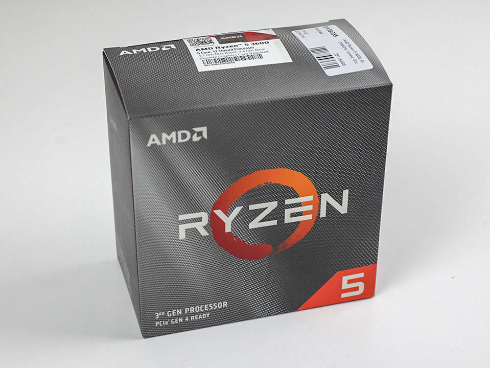
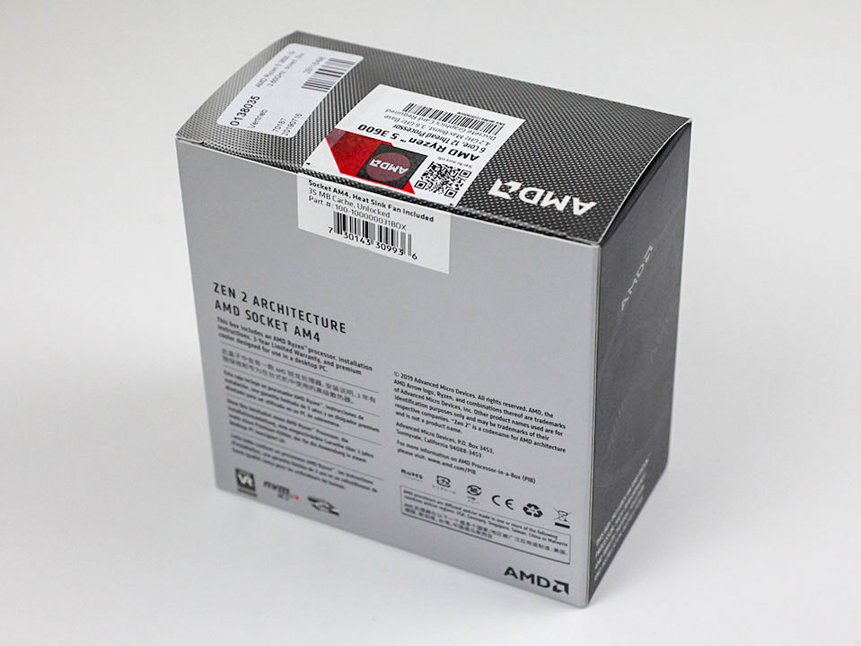
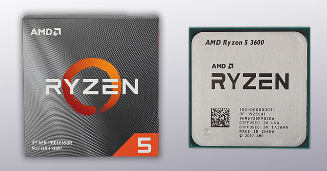
The Ryzen 5 3600 ships in cuboidal paperboard box with carbon-fiber texture on some of its faces. There are clear markings on the front that tell you this is a 3rd generation Ryzen processor, which has PCI-Express gen 4.0 support. The back also mentions "Zen 2". There are also some "VR ready" and NVMe logos on the box.


AMD includes a Wraith Stealth cooling solution suitable for the 65 W TDP of the Ryzen 5 3600.
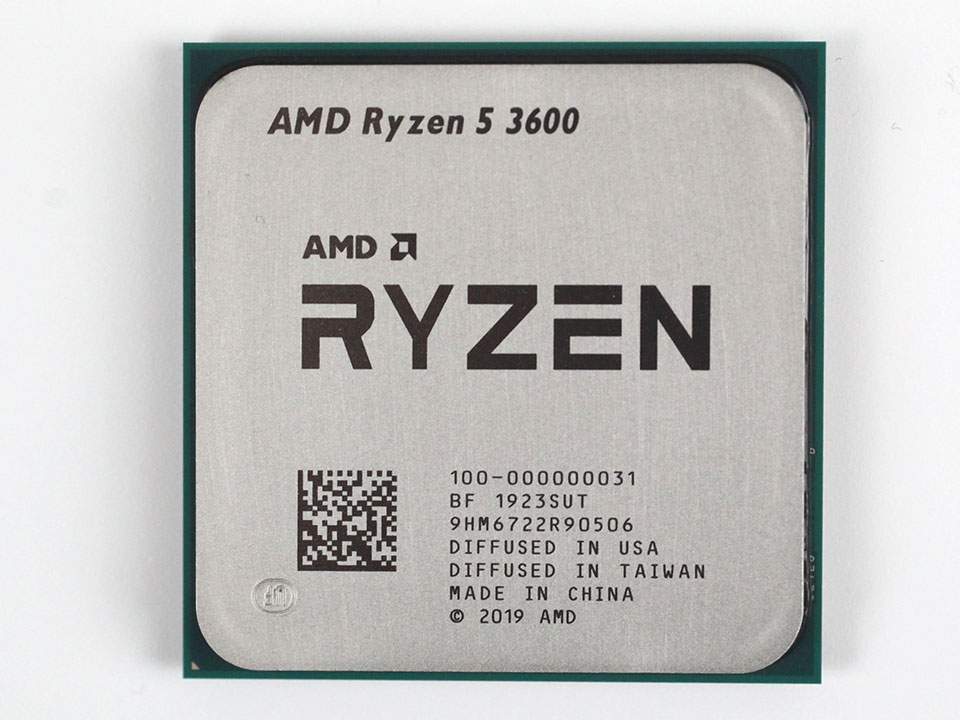

The Ryzen 5 3600 processor looks like any conventional AMD processor with a large IHS dominating the top, and a 1,331-pin micro-PGA in the bottom. You see national-origin markings for three places—USA, China, and Taiwan. The 7 nm "Zen 2" CPU chiplet is made at TSMC, Taiwan. The 12 nm I/O controller die is made in the US at GlobalFoundries. The two dies are packaged into the MCM at a facility in China.
Architecture

AMD's 3rd generation Ryzen processors use the "Zen 2" microarchitecture. The 2nd generation Ryzen chips use an enhanced first-generation "Zen" derivative called "Zen+", which has process and boost algorithm improvements eke out roughly a 4% IPC uplift. With "Zen 2", AMD's key design goal is to finally beat Intel in the IPC game. IPC, or instructions per clock, is loosely used to denote a CPU core's performance at a given clock speed. For the past 15 or so years, Intel dominated AMD at IPC, while AMD attempted to make their processors competitive by cramming in more CPU cores than Intel at any given price point for competitive multi-threaded performance. Today's software environment is increasingly multi-threaded, as are games. With "Zen 2", AMD set itself an ambitious double-digit-percentage IPC uplift target to catch up or overtake Intel's latest "Coffee Lake" microarchitecture at IPC. AMD didn't stop there and even increased core counts for the platform at higher price points. The 3rd generation Ryzen family even includes a 16-core processor, which is a tremendous core count for the mainstream-desktop platform.


Before we get into the interesting and quirky way AMD crammed 16 cores into this chip, let's talk about the "Zen 2" CPU core. After the colossal failure that was "Bulldozer," AMD set out to once again build strong and monolithic CPU cores that share nothing except L3 cache with other cores. It achieved this desired result with "Zen", which posted a mammoth 40%–50% IPC increase over "Bulldozer", catapulting AMD back into competitiveness. "Zen" cores IPC sits somewhere between "Haswell" and "Skylake/Coffee Lake", which was enough for AMD as it backed the IPC increase with higher core counts compared to Intel. Over the 8th and 9th generations of Core processors that retained the same IPC as "Skylake", Intel shored up core counts to match AMD. Wanting to set up a definitive edge over Intel, AMD not only worked to increase IPC, but also core counts.
The "Zen 2" CPU core has essentially the same component layout and hierarchy as "Zen", but with major changes and broadening of key components. As with "Zen" (or most x86 CPU cores), the "Zen 2" core is made up of five key components: Fetch, Decode, Integer, Floating-point, and load-store. Fetch and Decode tell the CPU core what needs to be done and what data or instructions are needed; Integer and Floating-Point Unit execute a mathematical model of what needs to be done depending on the data type and nature of the instruction; Load/Store are the I/O of the CPU core. At various levels, there are tiny buffers, registers that store instructions, and larger caches that cushion data-transfers between various components.
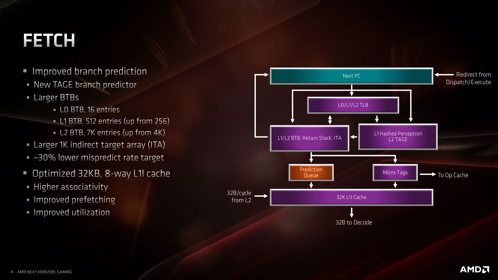

AMD updated the Fetch and Decode units, which contribute to IPC, by making the CPU work "smarter". The updated Integer and FPU make the CPU work "harder", the Load/Store unit's job is to make sure the other components aren't starved of things to do. The Fetch unit is updated with a TAGE branch predictor. Invented in 2006, TAGE is considered to be the best branch-prediction technique by the IEEE. AMD broadened the BTB (branch target buffers) at L1 and L2 by doubling the L1 entries to 512k, and L2 entries to 7,000 from 4,000. The ITA (indirect target array) has also been expanded. The design goal for updating the Fetch unit is to lower "mispredictions" (bad guesses) that wasted load/storage operations by 30 percent. The 32 KB L1 instruction cache has also been improved. The Decode unit has two improvements to the Op cache: improved instruction fusion and the ability to push up to 4,000 fused instructions per clock cycle.

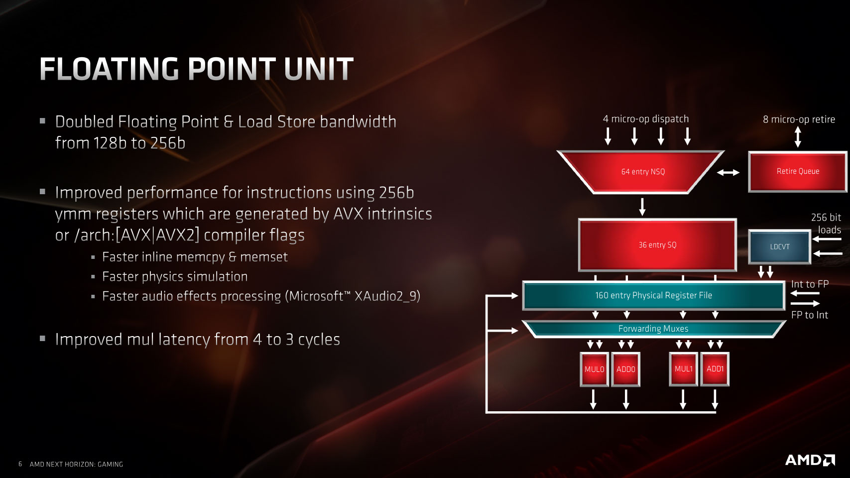
We now move on to the two components that contribute the most to the IPC, the Integer and Floating-point Units. The Integer unit receives incremental updates in the form of a broader integer scheduler that handles 92 entries (up from 84), with four 16-entry ALU queues and one 28-entry AGU queue. The general-purpose physical register file has now been expanded to 180 entries from 168. The issue-per-cycle has been broadened to 7 from 6, which now includes 4 ALUs and 3 AGUs. The reorder-buffer (ROB) has been broadened to 224 entries, up from 192. The SMT (simultaneous multi-threading) logic has been tweaked to better share the ALUs and AGUs among the logical processors. The FPU has the bulk of the innovation with "Zen 2". The load/store bandwidth of the FPU has been doubled to 256-bit, up from 128-bit on "Zen".
The core now also supports a sort of AVX-256: AVX/AVX2-flagged instructions with 256-bit registers. There are many applications for this, such as physics simulation, audio-stack execution, and memory-copy performance improvement. Multiplication operation latency has been improved by 33 percent.
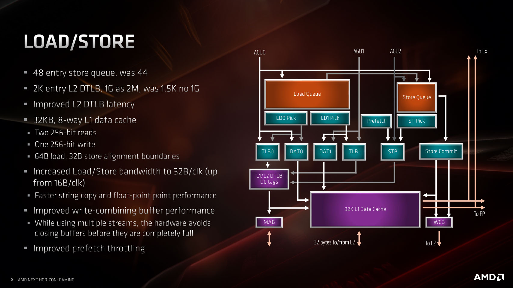
Lastly, we move on to the Load/Store unit with a similar round of generational enhancements. The entry-store queue is expanded to 48 entries, up from 44. The L2 TLB (translation lookaside buffer) has been expanded by 33% to 2,000 entries, and its latency improved. The 32 KB L1 Data cache has two 256-bit read paths and one 256-bit write path, with 64-byte load and 32-byte store alignment boundaries. The load/store bandwidth to L2 has been doubled to 32 bytes per clock.
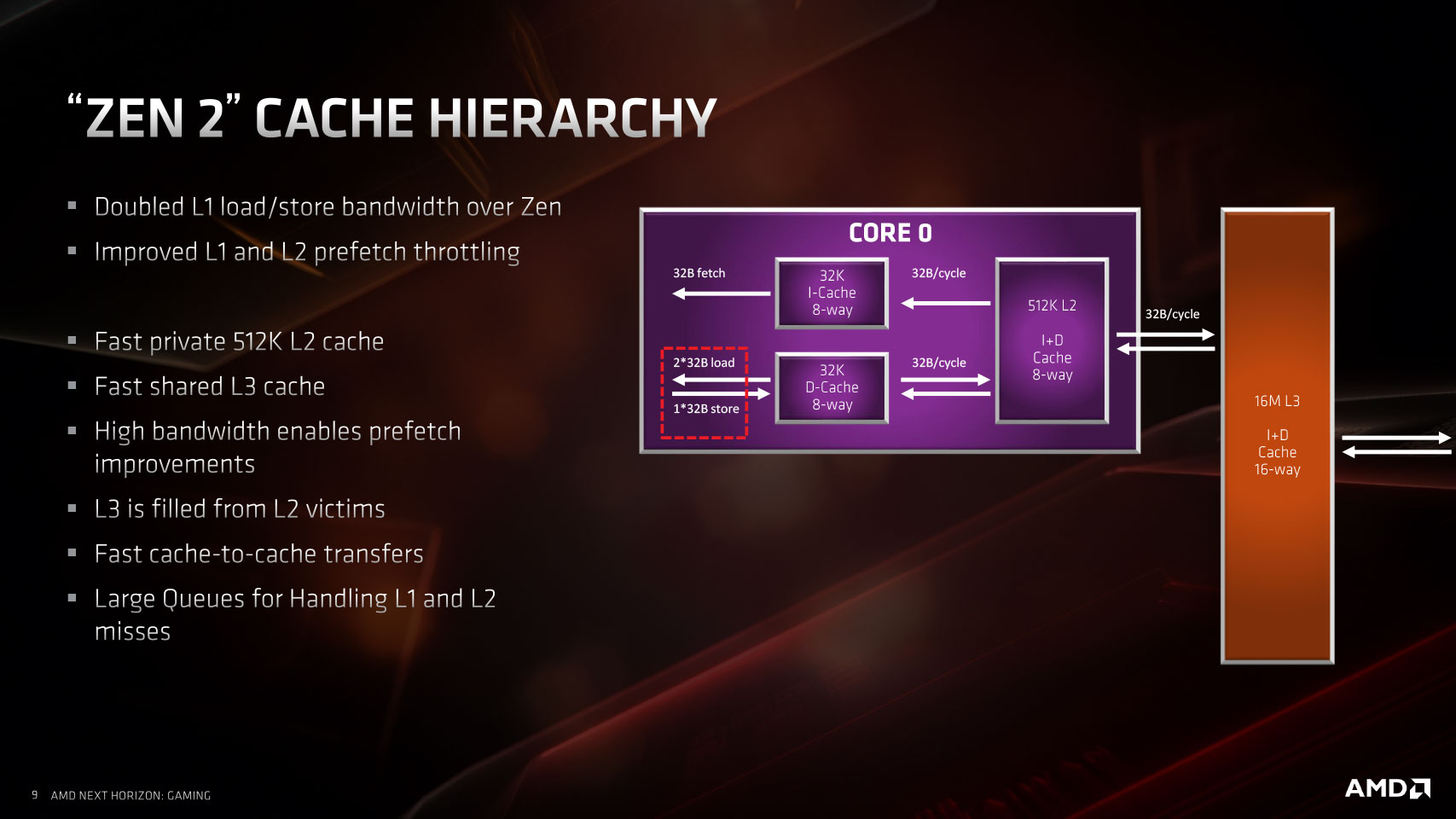
We now move on to the cache hierarchy, which is essentially the same as "Zen." Notwithstanding the technical changes described above, the "Zen 2" core still has a 32 KB 8-way L1I cache, a 32 KB 8-way L1D cache, and a dedicated 512 KB 8-way L2 cache. AMD doubled the shared L3 cache size to 16 MB. Every CCX (quad-core compute complex) on a "Zen 2" processor now has 16 MB of shared L3 cache. The doubling in L3 cache size was necessitated not just by Intel sharing larger amounts of L3 cache among individual cores on the "Coffee Lake Refresh" silicon (16 MB shared among all 8 cores), but also because the larger L3 cache on a "Zen 2" CCX cushions data transfers with the I/O controller die.

This brings us to the interesting and quirky way AMD achieved 16 cores. The Ryzen 9 3900X and Ryzen 5 3600 processor packages are codenamed "Matisse". This is a multi-chip module (MCM) of one or two 7 nm 8-core "Zen 2" CPU chiplets and one I/O controller die built on the 12 nm process. AMD made sure only those components that tangibly benefit from the shrink to 7 nm—namely, the CPU cores—are built on the new process, while those components that don't benefit from 7 nm stay on the existing 12 nm process, on the I/O controller die. AMD carved the Ryzen 5 3600 out by using just one "Zen 2" chiplet, and enabling 6 cores on it, 3 per CCX.

These components include the processor's dual-channel DDR4 memory controller, a 24-lane PCI-Express gen 4.0 root-complex, and an integrated southbridge that puts out some platform connectivity directly from the AM4 socket, such as SATA 6 Gbps and USB 3.1 ports. Infinity Fabric is the interconnect that binds the three dies by providing a 100 GB/s data path between each CPU chiplet and the I/O controller. The memory clock is now practically de-coupled from the Infinity Fabric clock, which should improve memory overclocking headroom. AMD also claims to have put in a lot of work to improving memory-module compatibility across brands, especially since Samsung stopped mass-production of the expensive B-die DRAM chip that favored AMD processors. The memory scaling article talks a little more about this.
AMD "Valhalla" X570 Desktop Platform

AMD delivered on its promise of 3rd generation Ryzen "Matisse" processors being backwards compatible with older socket AM4 motherboards, going all the way back to the AMD 300-series chipset with a simple BIOS update. To make the most out of Ryzen "Matisse"—namely, PCI-Express gen 4.0 connectivity and increased CPU/memory overclocking headroom, you're expected to use one of the latest motherboards that use the AMD X570 chipset. The X570 is an entirely different chip from the X470 and X370. Rather slim in their downstream connectivity, the older chipsets were supplied by ASMedia.
The X470 only puts out 8 PCIe gen 2.0 downstream lanes, for example. The X570 modernizes all I/O by putting out up to 16 PCIe gen 4.0 downstream lanes. This enables additional M.2 PCIe gen 4 slots on your motherboards for the latest SSDs featuring PCIe gen 4 support and creates room for many new bandwidth-hungry onboard devices, such as 10 GbE adapters, next-generation Thunderbolt, 802.11ax controllers, etc. Along with the "Matisse" SoC, the X570 also puts out a number of 10 Gbps USB 3.1 gen 2 ports. Motherboards based on X570 also implement modern network connectivity options, such as 2.5 GbE and 802.11ax WLAN.
Test Setup
| Test System "Zen 2" | |
|---|---|
| Processor: | All AMD Ryzen 3000 |
| Motherboard: | ASRock X570 Taichi AMD X570, BIOS v1.30 |
| Memory: | 2x 8 GB G.SKILL Flare X DDR4 DDR4-3200 14-14-14-34 |
| Graphics: | EVGA GeForce RTX 2080 Ti FTW3 Ultra |
| Storage: | 1 TB SSD |
| Power Supply: | Seasonic SS-860XP |
| Software: | Windows 10 Professional 64-bit Version 1903 (May 2019 Update) |
| Drivers: | NVIDIA GeForce 430.63 WHQL AMD Chipset 1.07.07.0725 |
| Test System "Zen" | |
|---|---|
| Processor: | All AMD Ryzen 2000, Ryzen 2000G and Ryzen 1000 |
| Motherboard: | MSI X470 Gaming M7 AC AMD X470, BIOS 7B77v19O |
| Memory: | 2x 8 GB G.SKILL Flare X DDR4 DDR4-3200 14-14-14-34 |
| Graphics: | EVGA GeForce RTX 2080 Ti FTW3 Ultra |
| Storage: | 1 TB SSD |
| Power Supply: | Seasonic SS-860XP |
| Software: | Windows 10 Professional 64-bit Version 1903 (May 2019 Update) |
| Drivers: | NVIDIA GeForce 430.63 WHQL AMD Chipset 1.07.07.0725 |
| Test System "Coffee Lake" | |
|---|---|
| Processor: | All Intel 8th & 9th Generation processors |
| Motherboard: | ASUS Z390 Maximus XI Extreme Intel Z390, BIOS 1105 |
| Memory: | 2x 8 GB G.SKILL Flare X DDR4 DDR4-3200 14-14-14-34 |
| Graphics: | EVGA GeForce RTX 2080 Ti FTW3 Ultra |
| Storage: | 1 TB SSD |
| Power Supply: | Seasonic SS-860XP |
| Software: | Windows 10 Professional 64-bit Version 1903 (May 2019 Update) |
| Drivers: | NVIDIA GeForce 430.63 WHQL |
- All applications, gamesm and processors are tested with the drivers and hardware listed above—no performance results were recycled between test systems.
- All games and applications are tested using the same game version.
- All games are set to their highest quality setting unless indicated otherwise.
Our Patreon Silver Supporters can read articles in single-page format.
Apr 1st, 2025 17:46 EDT
change timezone
Latest GPU Drivers
New Forum Posts
- Is the futureproof gaming solution a four drive system? (36)
- lowering the voltage but performance decreased a lot. (5)
- Asus Rampage IV Formula Bios MOD (NVME Support + Resizable BAR) (0)
- What do you do for a living? (473)
- RTX 3090 is still a good card? (15)
- Is RX 9070 VRAM temperature regular value or hotspot? (280)
- Question about Intel Optane SSDs (59)
- [Intel AX1xx/AX2xx/AX4xx/AX16xx/BE2xx/BE17xx] Intel Modded Wi-Fi Driver with Intel® Killer™ Features (300)
- What are you playing? (23331)
- 5090 is terrible (3)
Popular Reviews
- DDR5 CUDIMM Explained & Benched - The New Memory Standard
- Sapphire Radeon RX 9070 XT Pulse Review
- ASRock Phantom Gaming B850 Riptide Wi-Fi Review - Amazing Price/Performance
- SilverStone Lucid 04 Review
- Palit GeForce RTX 5070 GamingPro OC Review
- Samsung 9100 Pro 2 TB Review - The Best Gen 5 SSD
- Sapphire Radeon RX 9070 XT Nitro+ Review - Beating NVIDIA
- Enermax REVOLUTION D.F. 12 850 W Review
- Assassin's Creed Shadows Performance Benchmark Review - 30 GPUs Compared
- AMD Ryzen 7 9800X3D Review - The Best Gaming Processor
Controversial News Posts
- MSI Doesn't Plan Radeon RX 9000 Series GPUs, Skips AMD RDNA 4 Generation Entirely (146)
- Microsoft Introduces Copilot for Gaming (124)
- AMD Radeon RX 9070 XT Reportedly Outperforms RTX 5080 Through Undervolting (119)
- NVIDIA Reportedly Prepares GeForce RTX 5060 and RTX 5060 Ti Unveil Tomorrow (115)
- Over 200,000 Sold Radeon RX 9070 and RX 9070 XT GPUs? AMD Says No Number was Given (100)
- NVIDIA GeForce RTX 5050, RTX 5060, and RTX 5060 Ti Specifications Leak (96)
- Retailers Anticipate Increased Radeon RX 9070 Series Prices, After Initial Shipments of "MSRP" Models (90)
- China Develops Domestic EUV Tool, ASML Monopoly in Trouble (88)