 38
38
ASUS GeForce RTX 4060 Ti TUF OC Review
Test Setup »High-resolution PCB Pictures
These pictures are for the convenience of volt modders and people who would like to see all the finer details on the PCB. Feel free to link back to us and use these in your articles, videos or forum posts.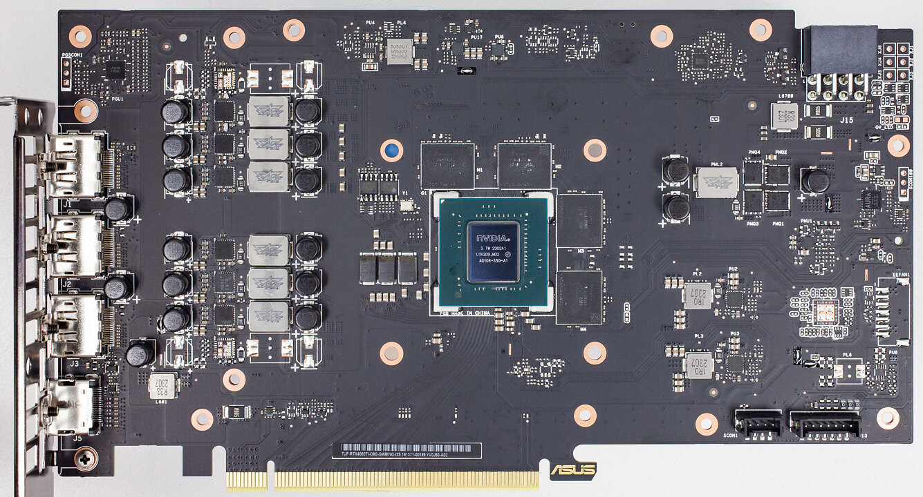

High-resolution versions are also available (front, back).
Circuit Board (PCB) Analysis
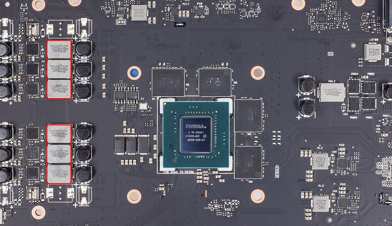
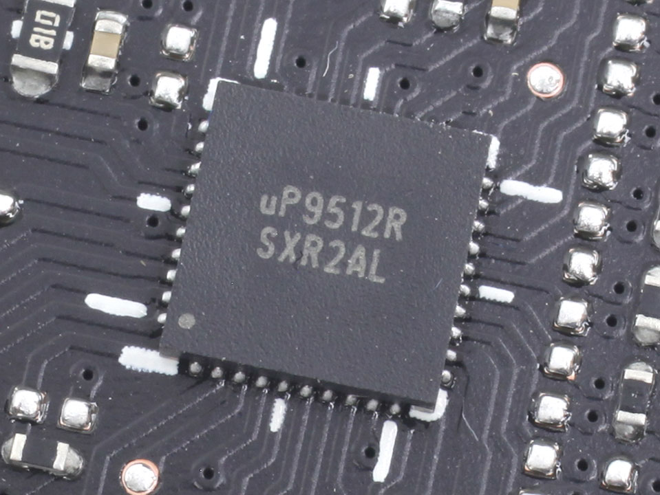
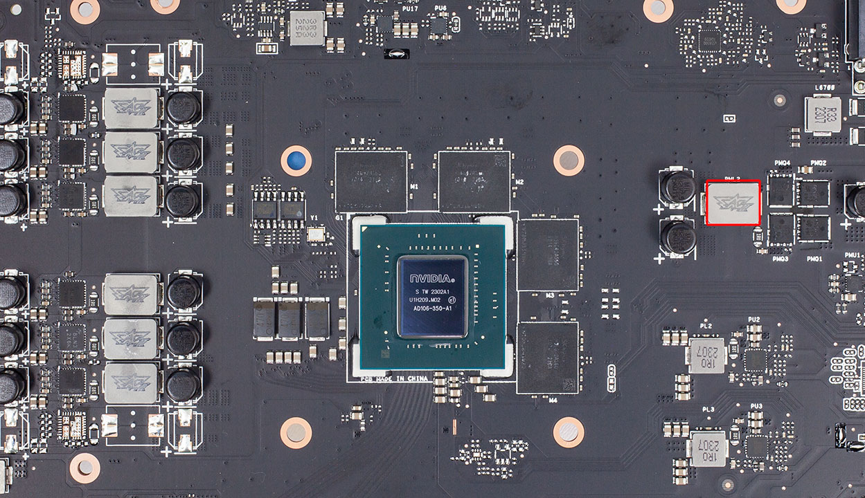
GPU voltage is handled by a 6-phase VRM driven by a UPI uP9512R controller.
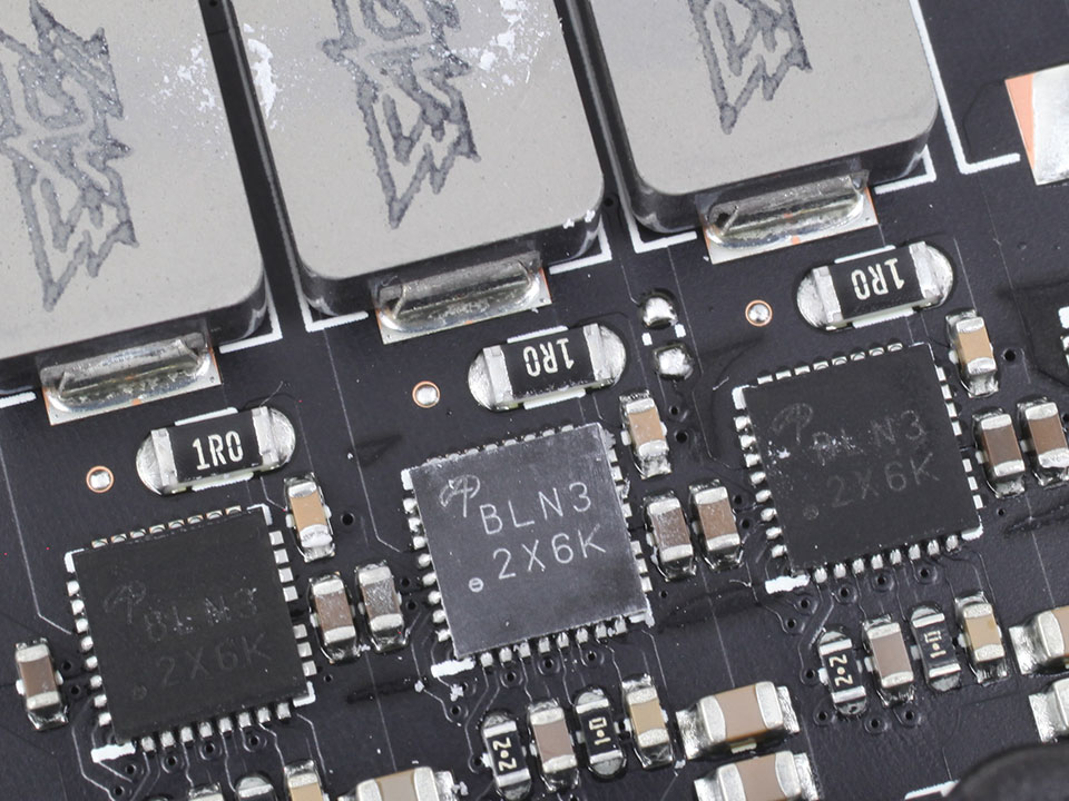
Alpha & Omega Semiconductor BLN3-AOZ5311NQI DrMOS are used for the GPU power phases, these are each capable of 55 A.
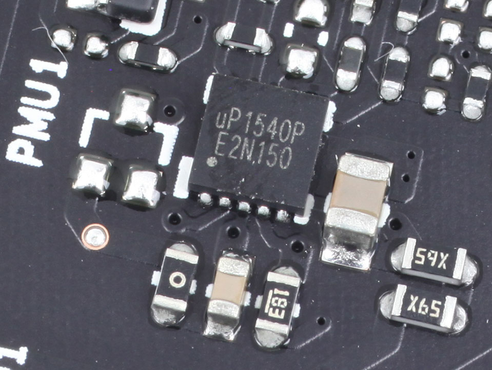
Memory voltage is a single-phase design, and handled by a UPI uP1540P controller.
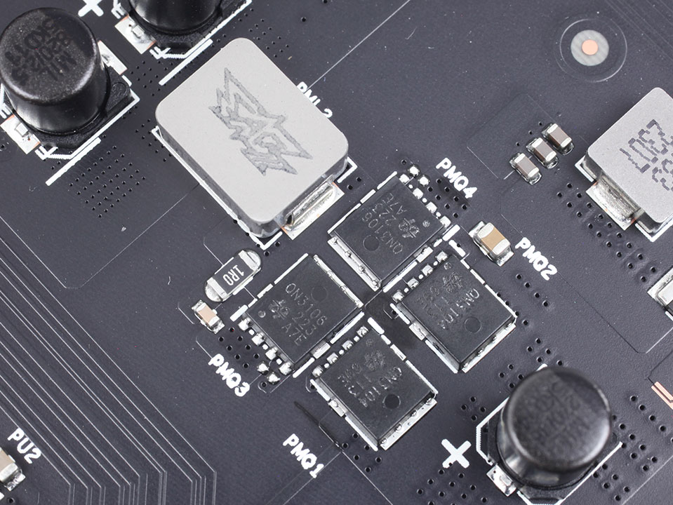
For memory, ASUS is using a set of Sinotech ON3106 and ON3104 discrete MOSFETs rated for 50 A.
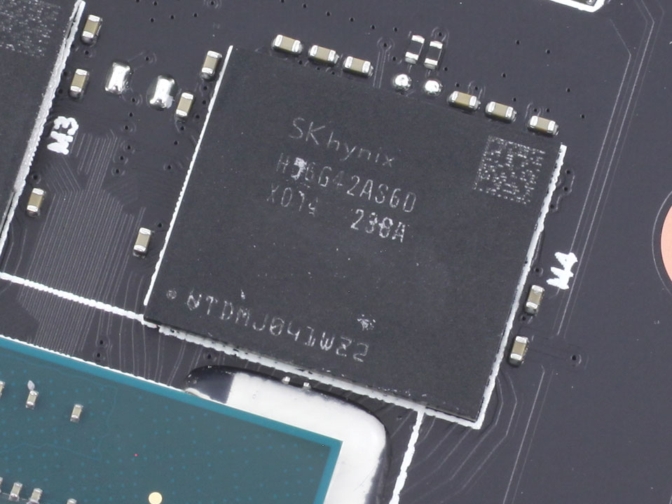
The GDDR6 memory chips are made by Hynix and carry the model number H56G42AS6DX-014. They are specified to run at 2250 MHz (18 Gbps effective).

NVIDIA's AD106 graphics processor is the company's fourth Ada Lovelace GPU. It is built using a 5 nanometer process at TSMC Taiwan, with a transistor count of 22.9 billion and a die size of 190 mm².
Jul 14th, 2025 15:44 CDT
change timezone
Latest GPU Drivers
New Forum Posts
- Stupid things one has done with hardware (47)
- No offense, here are some things that bother me about your understanding of fans. (109)
- AMD 7Ghz? This keeps popping up on my feeds! (5)
- Best motherboards for XP gaming (151)
- Which CPU to Choose for a 7900 XT? Ryzen 7 7700 or Ryzen 5 9600X? (43)
- Bent pins on an AM5 mobo, any way to test them and also find which ones were on the schematic? (6)
- i7 2860QM how to raise power limit? (20)
- Arc 770a 16gb money pit (9)
- Frametime spikes and stuttering after switching to AMD CPU? (572)
- What's your latest tech purchase? (24265)
Popular Reviews
- Lexar NM1090 Pro 4 TB Review
- Our Visit to the Hunter Super Computer
- MSI GeForce RTX 5060 Gaming OC Review
- Fractal Design Epoch RGB TG Review
- NVIDIA GeForce RTX 5050 8 GB Review
- Corsair FRAME 5000D RS Review
- Sapphire Radeon RX 9060 XT Pulse OC 16 GB Review - An Excellent Choice
- Chieftec Iceberg 360 Review
- AMD Ryzen 7 9800X3D Review - The Best Gaming Processor
- Upcoming Hardware Launches 2025 (Updated May 2025)
TPU on YouTube
Controversial News Posts
- Intel's Core Ultra 7 265K and 265KF CPUs Dip Below $250 (288)
- Some Intel Nova Lake CPUs Rumored to Challenge AMD's 3D V-Cache in Desktop Gaming (140)
- AMD Radeon RX 9070 XT Gains 9% Performance at 1440p with Latest Driver, Beats RTX 5070 Ti (131)
- NVIDIA Launches GeForce RTX 5050 for Desktops and Laptops, Starts at $249 (122)
- NVIDIA GeForce RTX 5080 SUPER Could Feature 24 GB Memory, Increased Power Limits (115)
- Microsoft Partners with AMD for Next-gen Xbox Hardware (105)
- Intel "Nova Lake‑S" Series: Seven SKUs, Up to 52 Cores and 150 W TDP (100)
- NVIDIA DLSS Transformer Cuts VRAM Usage by 20% (97)