 66
66
ASUS Maximus III Gene P55 Review
BIOS Walkthrough »The Board - A Closer Look

Next to the 24-pin ATX power connector, sits a fan header, and four little LEDs grouped together labelled Q_LED. The Q_LED lights indicate whether the items under each label have passed a POST test. CPU, DRAM, VGA, and BOOT_DEVICE each light up and turn off in the listed order as the board boots. They possess another function as well, as I noticed one blinking while in the OS, which happens to indicate whether a specific function of the board, MemPerfect, is in use. When this function is enabled, the DRAM LED will flash continually until it is disabled.
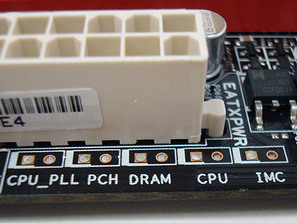
ASUS has included a set of voltage read points right next to the Q_LED section for those who want real-time accurate readings. The five read points, from right to left, include IMC(integrated memory controller), CPU (CPU core voltage), DRAM (memory), PCH (chipset), and finally, CPU PLL (clock source voltage). Each read point includes both positive and ground contact points to ensure a proper reading.
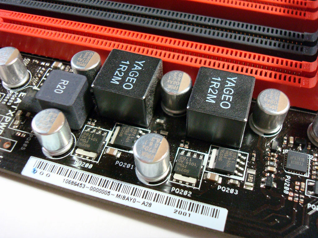
Next to the measure points are the two power phases for memory. The intelligent design used here is more than sufficient for ultra-high RAM clocking, even when using four sticks at high overclock speeds.
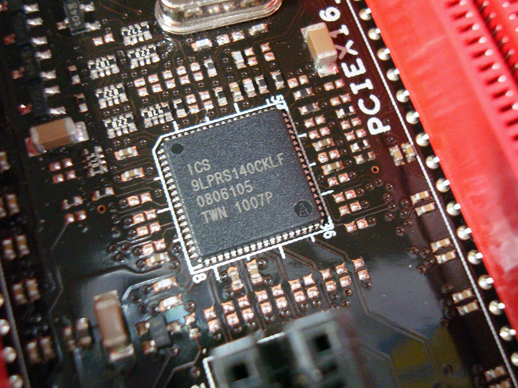
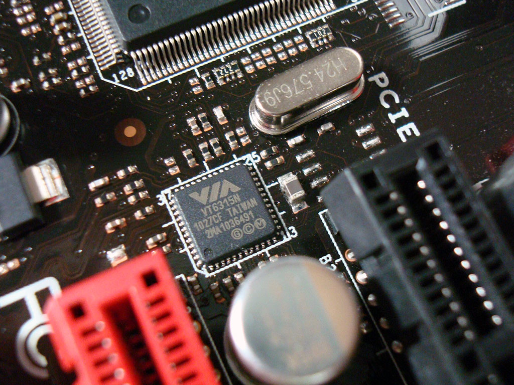
Moving between the PCI-E slots, we can see the ICS clock generator, responsible for generating all the clock frequencies for the board, CPU and periphery.
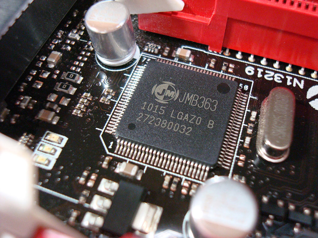
The JMicron JMB363 chipset adds extra optical and eSATA drive support.
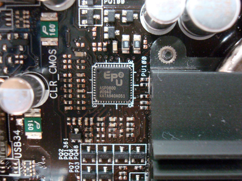
Moving back up to the edge of the CPU socket near the rear I/O, we find the EPU2 chip that controls the CPU power delivery system. This chip makes sure all phases are in use, or disabled in idle mode, it also monitors voltage and current supplied to the CPU.
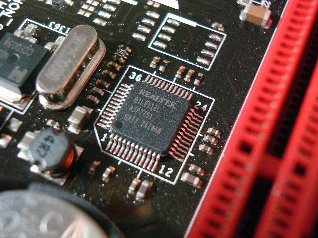
Above the slots sits the CMOS battery, with the Realtek LAN chip beside it. So much thought has gone into this board's design, that even the battery is removable with all slots populated. ASUS engineers have really done an awesome job with this board's layout.

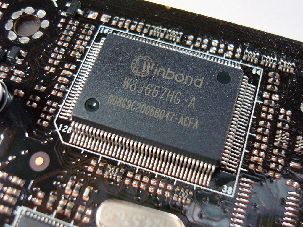
At the bottom left edge we find the VIA audio chip that supports the SupremeFX X-Fi, the Winbond SuperIO, and the VIA FireWire chipset. Unlike previous versions of this board, my sample does not have the silver “SupremeFX” metal cover over the audio section. A white CD-in, SPDIF-out, and front panel connector, are close by as well.
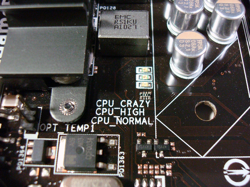
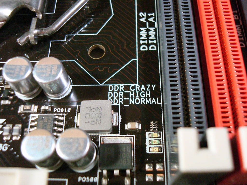
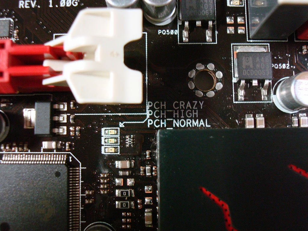
ASUS has also included a set of voltage indicator LEDs in various places around the board. The CPU, southbridge and the DDR3 memory slots each get a set of three LEDs; green, yellow, and red. Each color indicates a voltage range, and like traffic signals almost all of us are familiar with, green is "go", yellow is "caution", and red is "STOP! You are burning up my circuits!"
It all works out to be a lot of features. I am thoroughly impressed by everything ASUS has managed to squeeze into this board, and even more impressed with how uncluttered and clean the whole board appears. It really is a wolf in sheep's clothing. Or rather, a serious overclocking board, in MicroATX form-factor. Let's take a look at the BIOS, and see if that theme is matched there as well.
Jul 19th, 2025 01:05 CDT
change timezone
Latest GPU Drivers
New Forum Posts
- VMware Workstation is now free for personal use (20)
- What's your latest tech purchase? (24312)
- 9060 XT 8GB or 5060 8GB? (35)
- question for everyone about google play games beta (1)
- Gacha Games - Discussions, Pulls, Updates, etc. (0)
- Idle issue since 5060 ti installed (28)
- Windows 11 General Discussion (6151)
- Have you got pie today? (16795)
- Anime Nation (13054)
- Stalker 2 is looking great. (214)
Popular Reviews
- MSI GeForce RTX 5060 Gaming OC Review
- Razer Blade 16 (2025) Review - Thin, Light, Punchy, and Efficient
- Thermal Grizzly WireView Pro Review
- Pulsar X2 Crazylight Review
- SilverStone SETA H2 Review
- AVerMedia Live Gamer Ultra S (GC553Pro) Review
- Upcoming Hardware Launches 2025 (Updated May 2025)
- Sapphire Radeon RX 9060 XT Pulse OC 16 GB Review - An Excellent Choice
- NVIDIA GeForce RTX 5050 8 GB Review
- Our Visit to the Hunter Super Computer
TPU on YouTube
Controversial News Posts
- Intel's Core Ultra 7 265K and 265KF CPUs Dip Below $250 (288)
- Some Intel Nova Lake CPUs Rumored to Challenge AMD's 3D V-Cache in Desktop Gaming (140)
- AMD Radeon RX 9070 XT Gains 9% Performance at 1440p with Latest Driver, Beats RTX 5070 Ti (131)
- NVIDIA Launches GeForce RTX 5050 for Desktops and Laptops, Starts at $249 (124)
- NVIDIA GeForce RTX 5080 SUPER Could Feature 24 GB Memory, Increased Power Limits (115)
- Microsoft Partners with AMD for Next-gen Xbox Hardware (105)
- NVIDIA DLSS Transformer Cuts VRAM Usage by 20% (99)
- AMD Sampling Next-Gen Ryzen Desktop "Medusa Ridge," Sees Incremental IPC Upgrade, New cIOD (97)