 112
112
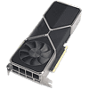
NVIDIA GeForce RTX 3080 Ti Founders Edition Review
Test Setup »High-resolution PCB Pictures
These pictures are for the convenience of volt modders and people who would like to see all the finer details on the PCB. Feel free to link back to us and use these in your articles, videos or forum posts.

High-res versions are also available (front, back).
Circuit Board (PCB) Analysis
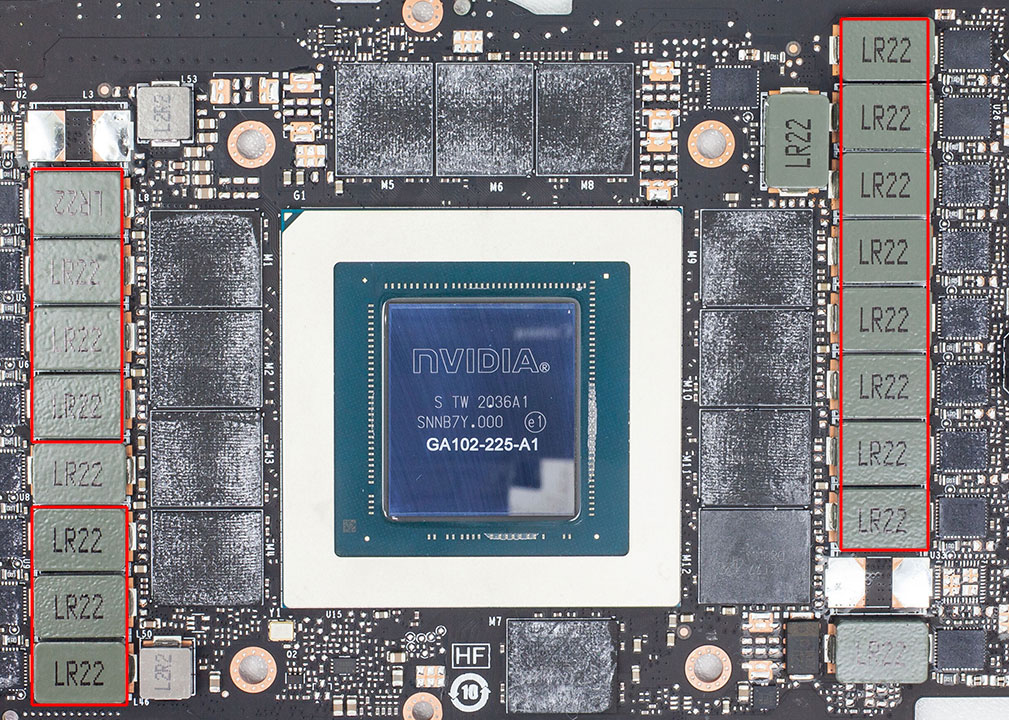


The GPU VRM is 15-phase, controlled by two voltage controllers. The Monolithic Power Systems MP2888B supports up to ten phases, and the MP2886B supports up to six phases.

Monolithic Power Systems MP86957 DrMOS are used for GPU voltage. These are rated for 70 A.


Memory voltage uses a three-phase design and is managed by a Monolithic System MP2884B.

For memory, MP86957 DrMOS chips are used, too.

The GDDR6X memory chips are made by Micron and carry the model number D8BWW, which decodes to MT61K256M32JE-19G:T. They are specified to run at 1188 MHz (19 Gbps GDDR6X effective).

NVIDIA's GA102 graphics processor is the company's second Ampere architecture chip, the first one targeted at GeForce gamers. It is produced on a 8 nanometer process at Samsung and has a transistor count of 28 billion with a die size of 628 mm².
Apr 1st, 2025 18:48 EDT
change timezone
Latest GPU Drivers
New Forum Posts
- RTX 3090 is still a good card? (18)
- Is RX 9070 VRAM temperature regular value or hotspot? (282)
- Post your cooling. (196)
- Wondering if I can keep the same cooler.. (1)
- Can you guess Which game it is? (55)
- lowering the voltage but performance decreased a lot. (6)
- Is the futureproof gaming solution a four drive system? (36)
- Asus Rampage IV Formula Bios MOD (NVME Support + Resizable BAR) (0)
- What do you do for a living? (473)
- Question about Intel Optane SSDs (59)
Popular Reviews
- DDR5 CUDIMM Explained & Benched - The New Memory Standard
- Sapphire Radeon RX 9070 XT Pulse Review
- ASRock Phantom Gaming B850 Riptide Wi-Fi Review - Amazing Price/Performance
- SilverStone Lucid 04 Review
- Palit GeForce RTX 5070 GamingPro OC Review
- Samsung 9100 Pro 2 TB Review - The Best Gen 5 SSD
- Sapphire Radeon RX 9070 XT Nitro+ Review - Beating NVIDIA
- Enermax REVOLUTION D.F. 12 850 W Review
- Assassin's Creed Shadows Performance Benchmark Review - 30 GPUs Compared
- AMD Ryzen 7 9800X3D Review - The Best Gaming Processor
Controversial News Posts
- MSI Doesn't Plan Radeon RX 9000 Series GPUs, Skips AMD RDNA 4 Generation Entirely (146)
- Microsoft Introduces Copilot for Gaming (124)
- AMD Radeon RX 9070 XT Reportedly Outperforms RTX 5080 Through Undervolting (119)
- NVIDIA Reportedly Prepares GeForce RTX 5060 and RTX 5060 Ti Unveil Tomorrow (115)
- Over 200,000 Sold Radeon RX 9070 and RX 9070 XT GPUs? AMD Says No Number was Given (100)
- NVIDIA GeForce RTX 5050, RTX 5060, and RTX 5060 Ti Specifications Leak (96)
- Retailers Anticipate Increased Radeon RX 9070 Series Prices, After Initial Shipments of "MSRP" Models (90)
- China Develops Domestic EUV Tool, ASML Monopoly in Trouble (88)