 540
540
Sapphire Radeon RX 9070 XT Nitro+ Review - Beating NVIDIA
Test Setup »High-resolution PCB Pictures
These pictures are for the convenience of volt modders and people who would like to see all the finer details on the PCB. Feel free to link back to us and use these in your articles, videos or forum posts.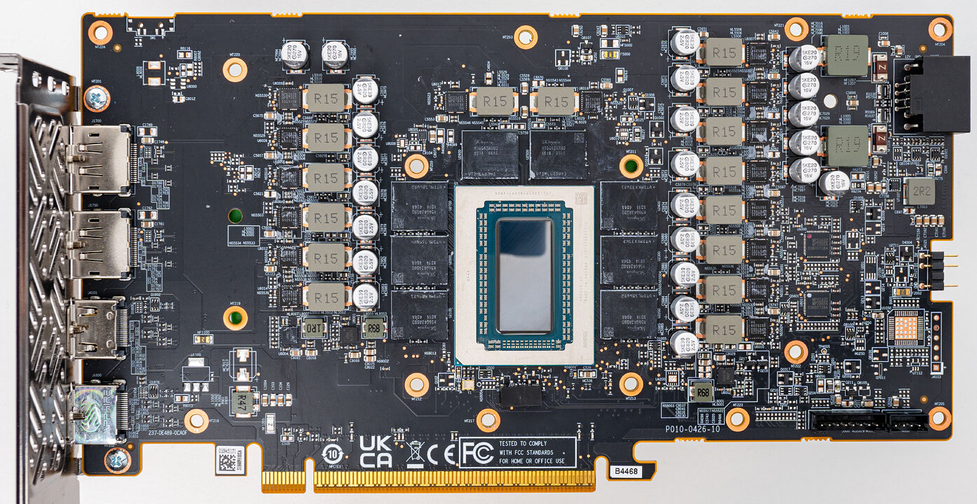
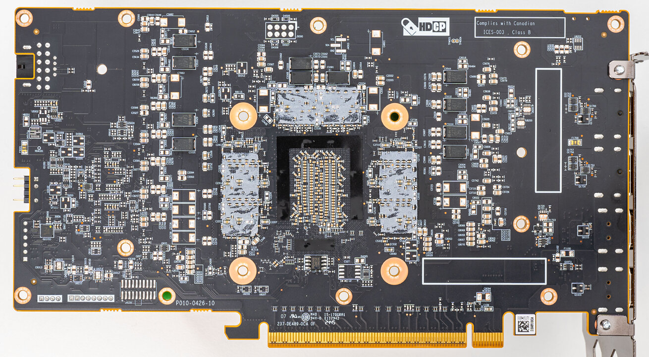
High-resolution versions are also available (front, back).
Circuit Board (PCB) Analysis
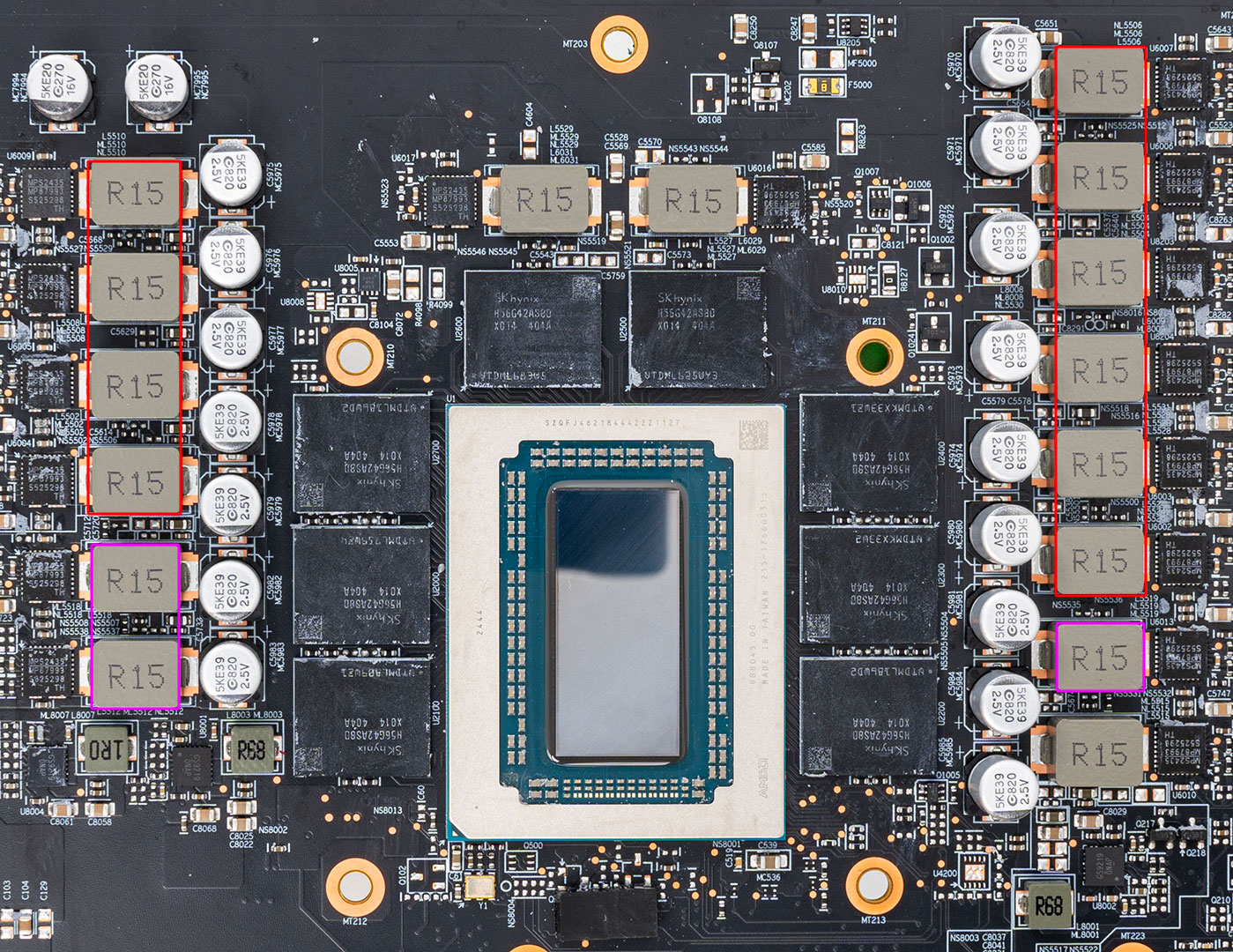
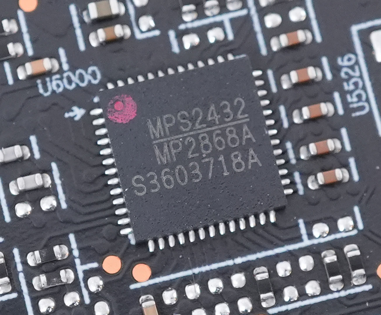
A 10+3 phase VRM powers the GPU. It is managed by a Monolithic Power Systems MP2868A controller.
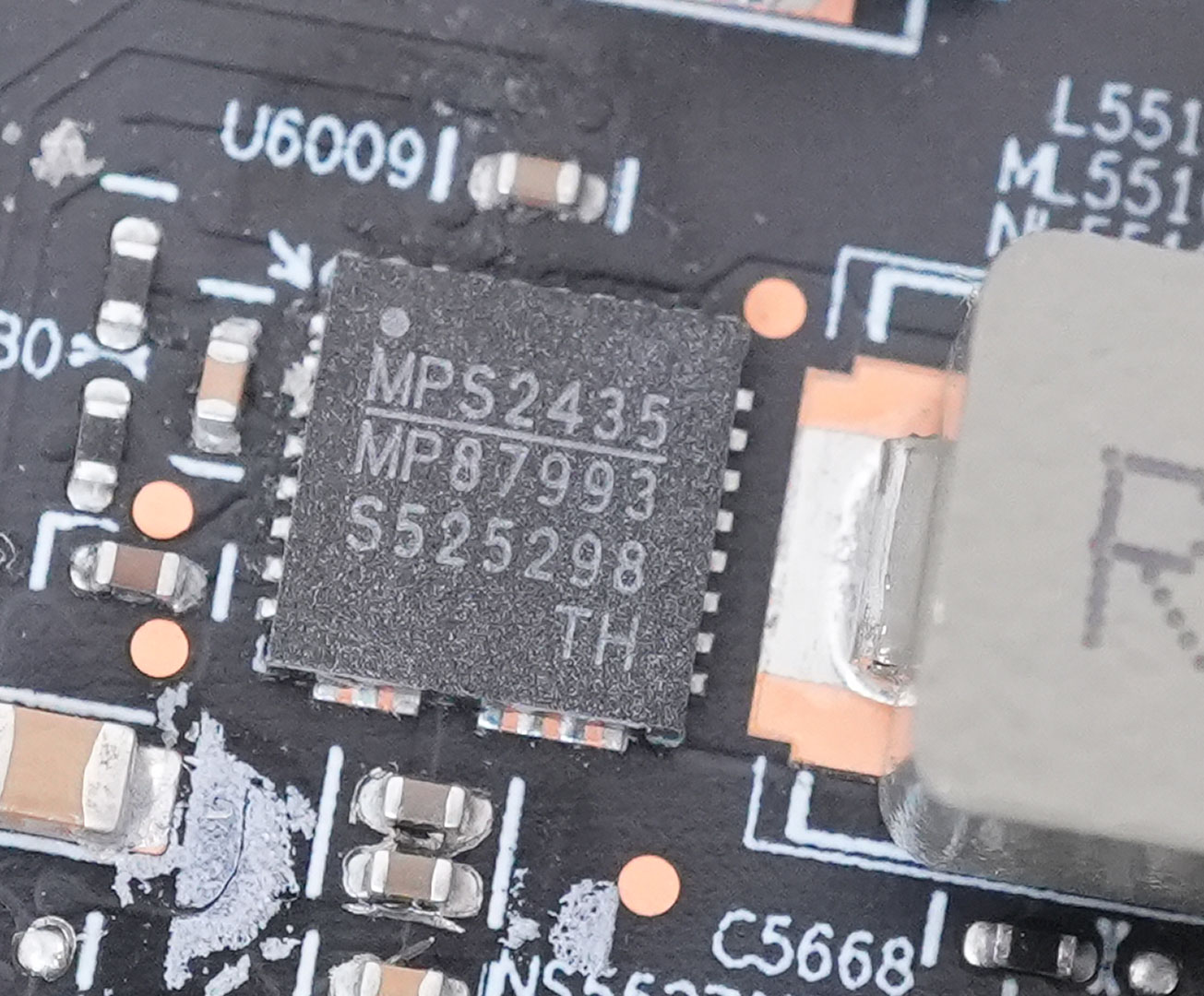
All GPU power phases use Monolithic MPS MP87993 DrMOS. These are new, we don't know their current rating. The "9" could suggest 90 A.
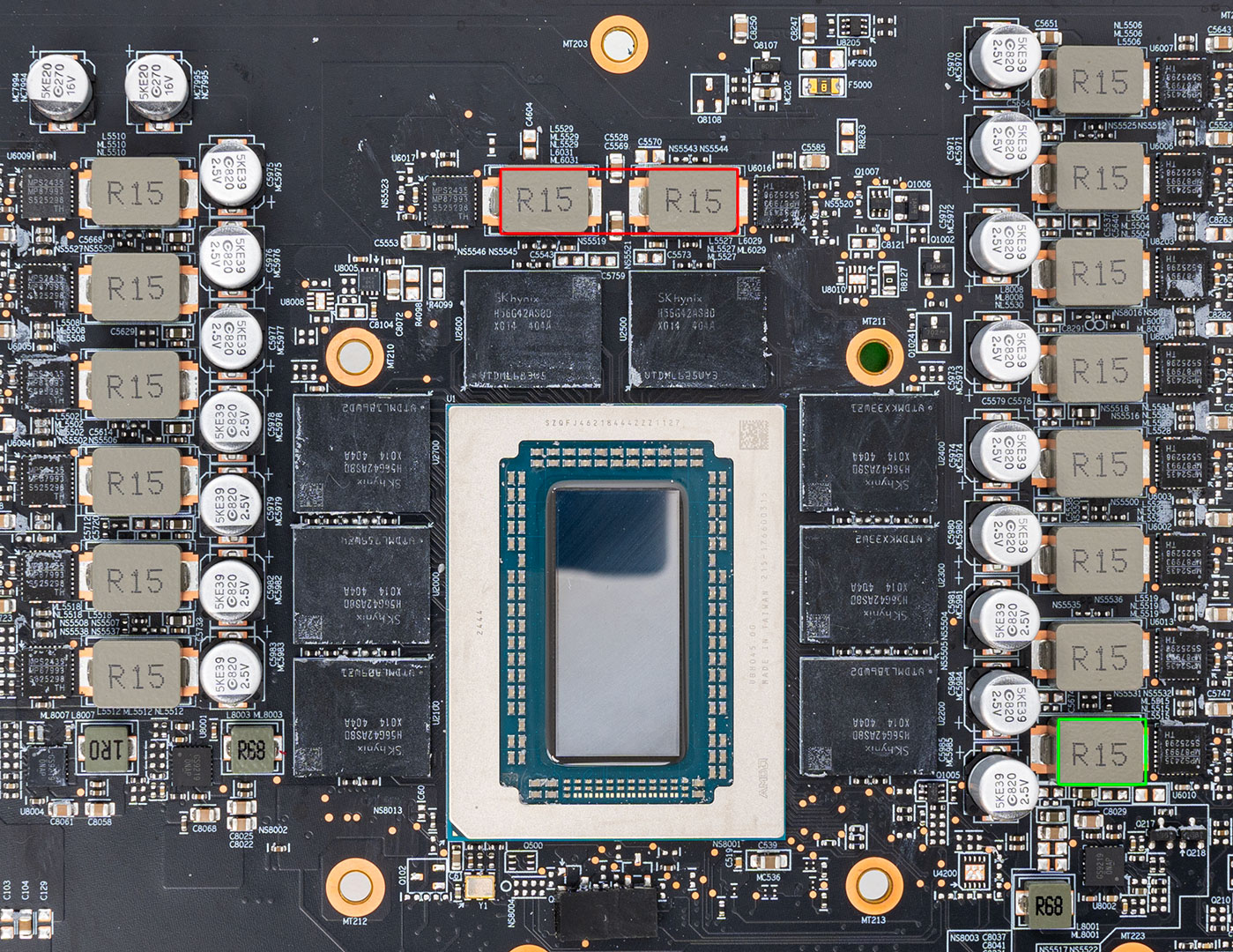
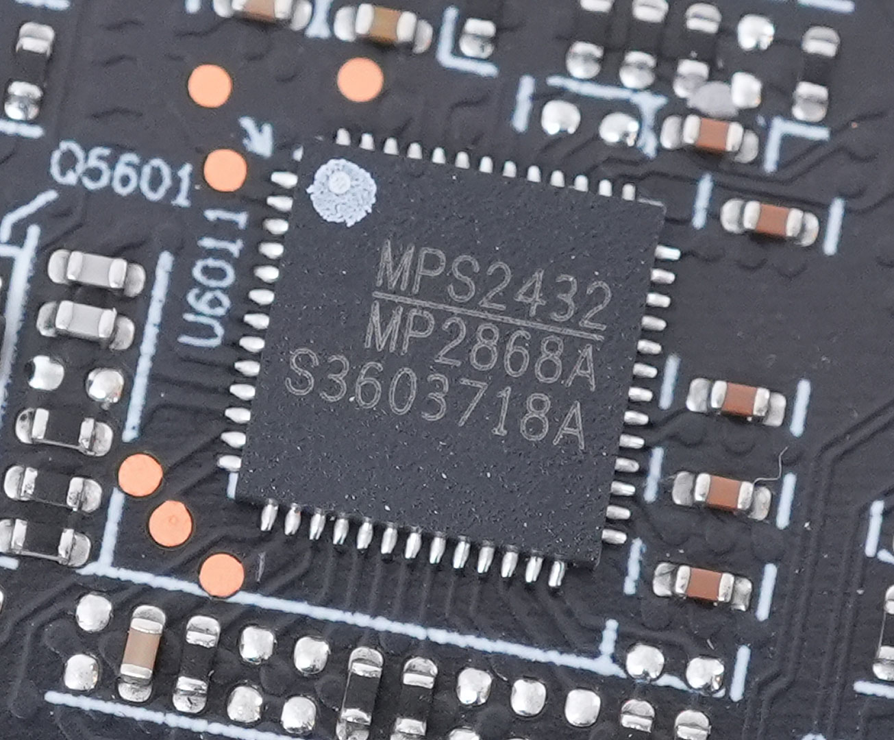
Powering the GDDR6 memory chips is a 3+1 phase VRM driven by a second Monolithic Power Systems MP2868A controller.

Just like GPU, the memory is handled by Monolithic MP87993 DrMOS chips.
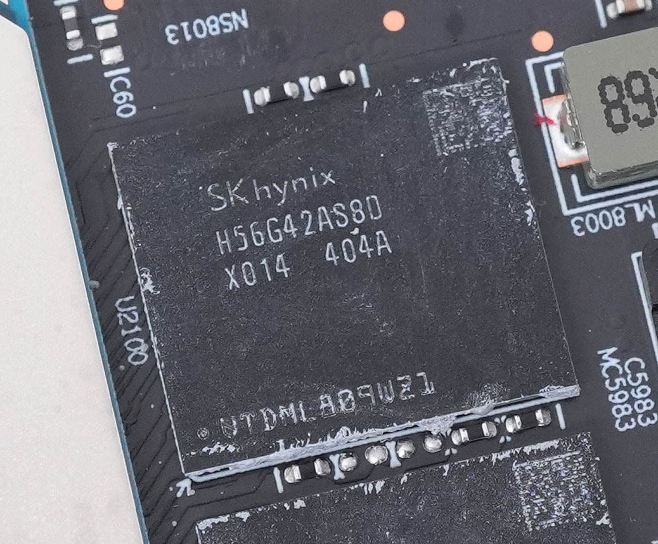
The GDDR6 memory chips are made by Hynix, and bear the model number H56G42AS8DX-014, they are rated for 20 Gbps.

The AMD Navi 48 GPU at the heart of the Radeon RX 9070 XT is a monolithic die. It is fabricated using a 4 nanometer N4P process at TSMC Taiwan. The die measures 357 mm², and comes with a transistor count of 53.9 billion.
Mar 6th, 2025 13:32 EST
change timezone
Latest GPU Drivers
New Forum Posts
- Free Games Thread (4533)
- 5070 Ti power limit questions (1)
- i5-8365U Fujitsu Lifebook Throttlestop (5)
- intel 1700 with high speed ram,memory (32)
- *Severe micro stutters* cyberpunk 2077 Please help (28)
- Questions about 5090 SUPRIM LIQUID (0)
- Microcenter GPU Stock status (25)
- Get 9070 or 9070 XT (87)
- My RX6800XT is not giving image anymore, Please Help. (8)
- getting ready for dual 5090, Functional protype on dual 4090 (76)
Popular Reviews
- Sapphire Radeon RX 9070 XT Nitro+ Review - Beating NVIDIA
- NVIDIA GeForce RTX 5070 Founders Edition Review
- ASUS Radeon RX 9070 TUF OC Review
- AMD Radeon RX 9070 Series Technical Deep Dive
- EIZO FlexScan EV4340X Review - A Multitasking Powerhouse
- RAWM ES21M Review
- ASUS GeForce RTX 5070 Ti TUF OC Review
- AMD Ryzen 7 9800X3D Review - The Best Gaming Processor
- Corsair Vengeance RGB CUDIMM DDR5-8800 48 GB CL42 Review
- MSI GeForce RTX 5070 Ti Vanguard SOC Review
Controversial News Posts
- NVIDIA GeForce RTX 50 Cards Spotted with Missing ROPs, NVIDIA Confirms the Issue, Multiple Vendors Affected (513)
- AMD Plans Aggressive Price Competition with Radeon RX 9000 Series (277)
- AMD Radeon RX 9070 and 9070 XT Listed On Amazon - One Buyer Snags a Unit (261)
- AMD Mentions Sub-$700 Pricing for Radeon RX 9070 GPU Series, Looks Like NV Minus $50 Again (248)
- AMD RDNA 4 and Radeon RX 9070 Series Unveiled: $549 & $599 (245)
- NVIDIA Investigates GeForce RTX 50 Series "Blackwell" Black Screen and BSOD Issues (244)
- AMD Radeon RX 9070 and 9070 XT Official Performance Metrics Leaked, +42% 4K Performance Over Radeon RX 7900 GRE (195)
- AMD Radeon RX 9070-series Pricing Leaks Courtesy of MicroCenter (158)