Monday, November 16th 2009

Radeon HD 5970 Offers Massive Overclocking Headroom
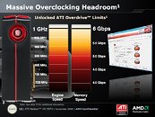
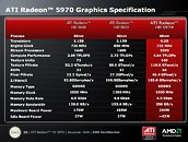
AMD's dual-GPU flagship graphics accelerator, the Radeon HD 5970, is closer than you think it is. Slated for 18th Nov, it includes every feature that allows AMD to reclaim the performance leadership it yearned for since the beginning of this year. In a series of company slides sourced from XtremeSystems Forums, it is learned that this could be one of the first accelerators which AMD "openly" markets as having a "Massive Headroom" for overclocking. While the clock speeds on the HD 5970 are lower than those on the single-GPU HD 5870, AMD lifted limits on what the driver-level ATI Overdrive software can offer in terms of clock speeds. While the engine (core) and memory speeds are set at 720/1000 MHz, the unlocked ATI Overdrive lets users take the clock speeds all the way up to 1000/1500 MHz. That's 30% for the core, and a stellar 50% for the memory.
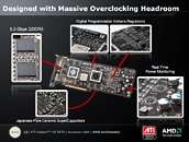
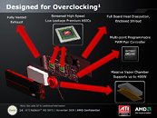
To back such speeds, AMD seems to have splurged heavily on top-notch components on the PCB. To begin with, the PCB holds two high-grade AMD Cypress GPUs, each with all its 1600 stream processors enabled. The GDDR5 memory, while clocked at 1000 MHz or 4 GT/s, is technically rated by its manufacturer to run at 1250 MHz or 5 GT/s. All systems are powered by high-grade digital PWM voltage regulators, with independent Volterra VRM controllers that allow real-time monitoring, and software voltage control. Barring the five-odd cylindrical solid-state capacitors, Japanese pure ceramic surface-mount capacitors are extensively made use of.The card's cooling assembly isn't any less descriptive either. It consists of a back-plate that cools memory chips on the reverse side of the PCB, while its obverse side is cooled by a large, consistent vapor-chamber plate, which covers the main components such as GPUs, the PCI-Express bridge chip, and the VRM chips. This is a design change compared to the R700 and R680, in which each GPU had its own heatsink, and one of the two would end up with second-hand (pre-heated) air from the other. Instead, the vapor-chamber plate conveys heat directly to a large, monolithic heatsink, which from the looks of it, features aluminum-fabbed air-channels. AMD's workhorse leaf-blower is still around, though this time, it is controlled by an SMSC EMC-2103 multi-point programmable PWM fan controller. The specs sheet shows the card's idle and maximum board power draws to be 42W and 294W, respectively.
Source:
XtremeSystems Forums
To back such speeds, AMD seems to have splurged heavily on top-notch components on the PCB. To begin with, the PCB holds two high-grade AMD Cypress GPUs, each with all its 1600 stream processors enabled. The GDDR5 memory, while clocked at 1000 MHz or 4 GT/s, is technically rated by its manufacturer to run at 1250 MHz or 5 GT/s. All systems are powered by high-grade digital PWM voltage regulators, with independent Volterra VRM controllers that allow real-time monitoring, and software voltage control. Barring the five-odd cylindrical solid-state capacitors, Japanese pure ceramic surface-mount capacitors are extensively made use of.The card's cooling assembly isn't any less descriptive either. It consists of a back-plate that cools memory chips on the reverse side of the PCB, while its obverse side is cooled by a large, consistent vapor-chamber plate, which covers the main components such as GPUs, the PCI-Express bridge chip, and the VRM chips. This is a design change compared to the R700 and R680, in which each GPU had its own heatsink, and one of the two would end up with second-hand (pre-heated) air from the other. Instead, the vapor-chamber plate conveys heat directly to a large, monolithic heatsink, which from the looks of it, features aluminum-fabbed air-channels. AMD's workhorse leaf-blower is still around, though this time, it is controlled by an SMSC EMC-2103 multi-point programmable PWM fan controller. The specs sheet shows the card's idle and maximum board power draws to be 42W and 294W, respectively.


90 Comments on Radeon HD 5970 Offers Massive Overclocking Headroom
i like on the graph for the hawx test for the nvidia bar it just says FAIL! lol that made me laugh
Still an amazing card though. Just in time for the Christmas rush too.
1 x 8 pin = 150 watts
1 x 6 pin = 75 watts
PCI-e power = 75 watts
300 watts total and max power usage at stock clocks is 294 watts. So where are the extra watts coming from to overclock this thing? There is a reason that they downclocked it to only 5850 speeds.
A question for those who know these things... With an 8+6 pin connectors would that be enough to supply 1.3v to each GPU? Just thinking about the ASUS voltage tweek cards and reading that 1.3v is about the practical limit. Or should someone who seriously wants to OC this card wait until someone comes out with one that has 8+8 pin connectors?
Giant vapor chamber FTW.
If ATi has released cards on this level now, and the rumors of them holding GT300 killers (5790s, 5890s & 5990s) in hand are true, waiting for their nVidia, in order to counter-launch, those must be just beyond words!:rockout:
Just yesterday there were celebrations about the first GPU with TeraFLOP performance, now we're already at 5!:eek:
if an intel cpu is specced to 3 ghz and you can run it at 4.5g you dont ask "where do the mhz come from?"
While OC headroom does seem gimmicky, its good to know for the enthusiasts out there (me :))
also good to know solidly from ATi themselves 5870CF is decently superior as of yet, and god I hope they drop prices on the 58's to release this at $499, that would MAKE MY DAY.
Gonna be mega fast! Anyone know uk prices yet?