Monday, November 16th 2009

Radeon HD 5970 Offers Massive Overclocking Headroom
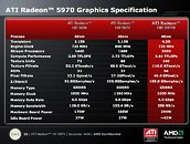
AMD's dual-GPU flagship graphics accelerator, the Radeon HD 5970, is closer than you think it is. Slated for 18th Nov, it includes every feature that allows AMD to reclaim the performance leadership it yearned for since the beginning of this year. In a series of company slides sourced from XtremeSystems Forums, it is learned that this could be one of the first accelerators which AMD "openly" markets as having a "Massive Headroom" for overclocking. While the clock speeds on the HD 5970 are lower than those on the single-GPU HD 5870, AMD lifted limits on what the driver-level ATI Overdrive software can offer in terms of clock speeds. While the engine (core) and memory speeds are set at 720/1000 MHz, the unlocked ATI Overdrive lets users take the clock speeds all the way up to 1000/1500 MHz. That's 30% for the core, and a stellar 50% for the memory.
To back such speeds, AMD seems to have splurged heavily on top-notch components on the PCB. To begin with, the PCB holds two high-grade AMD Cypress GPUs, each with all its 1600 stream processors enabled. The GDDR5 memory, while clocked at 1000 MHz or 4 GT/s, is technically rated by its manufacturer to run at 1250 MHz or 5 GT/s. All systems are powered by high-grade digital PWM voltage regulators, with independent Volterra VRM controllers that allow real-time monitoring, and software voltage control. Barring the five-odd cylindrical solid-state capacitors, Japanese pure ceramic surface-mount capacitors are extensively made use of.The card's cooling assembly isn't any less descriptive either. It consists of a back-plate that cools memory chips on the reverse side of the PCB, while its obverse side is cooled by a large, consistent vapor-chamber plate, which covers the main components such as GPUs, the PCI-Express bridge chip, and the VRM chips. This is a design change compared to the R700 and R680, in which each GPU had its own heatsink, and one of the two would end up with second-hand (pre-heated) air from the other. Instead, the vapor-chamber plate conveys heat directly to a large, monolithic heatsink, which from the looks of it, features aluminum-fabbed air-channels. AMD's workhorse leaf-blower is still around, though this time, it is controlled by an SMSC EMC-2103 multi-point programmable PWM fan controller. The specs sheet shows the card's idle and maximum board power draws to be 42W and 294W, respectively.
Source:
XtremeSystems Forums
To back such speeds, AMD seems to have splurged heavily on top-notch components on the PCB. To begin with, the PCB holds two high-grade AMD Cypress GPUs, each with all its 1600 stream processors enabled. The GDDR5 memory, while clocked at 1000 MHz or 4 GT/s, is technically rated by its manufacturer to run at 1250 MHz or 5 GT/s. All systems are powered by high-grade digital PWM voltage regulators, with independent Volterra VRM controllers that allow real-time monitoring, and software voltage control. Barring the five-odd cylindrical solid-state capacitors, Japanese pure ceramic surface-mount capacitors are extensively made use of.The card's cooling assembly isn't any less descriptive either. It consists of a back-plate that cools memory chips on the reverse side of the PCB, while its obverse side is cooled by a large, consistent vapor-chamber plate, which covers the main components such as GPUs, the PCI-Express bridge chip, and the VRM chips. This is a design change compared to the R700 and R680, in which each GPU had its own heatsink, and one of the two would end up with second-hand (pre-heated) air from the other. Instead, the vapor-chamber plate conveys heat directly to a large, monolithic heatsink, which from the looks of it, features aluminum-fabbed air-channels. AMD's workhorse leaf-blower is still around, though this time, it is controlled by an SMSC EMC-2103 multi-point programmable PWM fan controller. The specs sheet shows the card's idle and maximum board power draws to be 42W and 294W, respectively.


90 Comments on Radeon HD 5970 Offers Massive Overclocking Headroom
I can only imagine what they are conjuring up. :shadedshu
Ati has its day now but we ALL know what this means....
80 minutes for the reviews.
www.guru3d.com/article/radeon-hd-5970-review-test/
sorry for censoring out the box, it's not relevant for this, it's just convenient because it lets me connect 1 or 2 6 or 8-pin to 2x6 and 1x8pin.
"The PCI Express specification calls for a maximum provision of 300W for graphics, both HD 4870 X2 and HD 5970 max this specification out. With the Cypress GPU, though, we knew it would be require more power than RV770 becuase it was designed as a bigger chip; when designing the HF 5970 we had two options - keep within the specification and the standard infrastructure that exists (and tune the voltages and speeds accordingly) or break the infrascturcture and go beyond the specification. In the end we chose a hybrid - the default speeds are designed to fit within the spec and the default infrastucture, but we designed the board to facilitate higher current draws and allow users with higher quality power supplies to tweak the performance more. Can we guarantee OC specs? No, we can't, but we can say that the GPU's on those boards are screened to be high speed capable. "
Dave Baumann ATII never asked you to take my word for it try some independent research and thought. A lot of people have experience that doesn't mean you should never question their information or results or ask for evidence. I have a lot of respect for W1zzard and this website I didn't say he sucked but I still think the analogy was inappropriate.
How can it draw so much power, 150+75 doesn't = 270-280.
Sorry for slightly off topic but it is sort of relevant to the PCI-E power cable discussion.
That's why I was asking how can it be possible.
Not because I don't understand how current works.
Anyway back to topic :D