Tuesday, February 9th 2010

AMD to Sample 32 nm Processors Within H1 2010
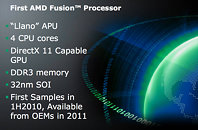
AMD, in its presentation at the International Solid State Circuits Conference (ISSCC) 2010, presented its plan to build its much talked about 'Fusion' processor platform, codenamed Llano, central to which, is the Accelerated Processing Unit (APU). AMD's APU is expected to be the first design to embed a multi-core x86 CPU and a GPU onto a single die. This design goes a notch ahead of Intel's recently released 'Clarkdale' processor, where Intel strapped a 32 nm dual-core CPU die and a 45 nm northbridge die with integrated graphics, onto an MCM (multi chip module) package. Llano is also expected to feature four processing cores, along with other design innovations.
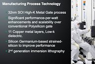
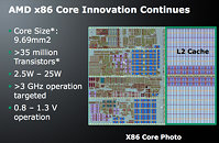
Some of the most notable announcements in AMD's presentation is that the company will begin sampling the chip to its industry partners within the first half of 2010. The Llano die will be build on a 32 nm High-K Metal Gate process. On this process, each x86 core will be as small as 9.69 mm². Other important components on the Llano die are a DDR3 memory controller, on-die northbridge, and a DirectX 11 compliant graphics core derived from the Evergreen family of GPUs. The x86 cores are expected to run at speeds of over 3 GHz. Each core has 1 MB of dedicated L2 cache, taking the total chip cache size to 4 MB.AMD has also embraced some new power management technologies, including power gating. Power gating is a feature that allows the system to power down some x86 core to push their power draw to near-zero. This reduces the chip's overall power draw better, which also allows active cores to be powered up. Similar to Intel's Turbo Boost technology. The power aware clock grid design reduces power consumption by cutting down on clock distribution across the chip.
With the APU, AMD thinks it has the right product for tomorrow's market, a chip which packs a large chunk of the motherboard's silicon, while not compromising on the features due to space constraints within the package. There's room made for four processing cores, and an Evergreen-derived DirectX 11 compliant GPU. If implemented well enough on the software side, AMD believes it can deliver one chip that handles both serial processing workloads (by the x86 cores), and highly parallel workloads (by the stream processors). Market availability of the chip isn't definitively known, but we expect it to be out early next year, or late this year.


46 Comments on AMD to Sample 32 nm Processors Within H1 2010
Wheres the level 3 cache?
Wheres the new powerful processing architecture to take on nehalem.
I sure as hell hope AMD has these things in mind for the fusion series.
Do some more searchin ;)
The biggest reason that consoles dominate the market for gaming is due to the fact that NONE of the integrated GPU's can run a game worth a darn. You combine this with the myth that "PC gaming is expensive" and you can see why we've been relegated to second-class citizens as far as gaming goes. If AMD can put out a chip that matches or exceeds the Clarkdale 660's GPU across both the desktop and mobile platforms, and manage to sell it at a cost that makes it too irresistible to pass up, then we may see a resurgence of PC gaming again.
For those saying "Integrated graphics?? LOL! L00zers!" are not helping on this. We need to get more people back to the PC for gaming otherwise you can rest assured we'll get more of the following:
a. DLC that nickles and dimes you for every frigging piece of content. Take Dragon Age where it got in your face about it during the game which is why I never picked it up.
b. Online only gaming service, like what Ubisoft announced, that forces PC users to stay online to play their games compared to consoles.
c. Console ports of titles where the field-of-view is locked to 60.
I could go on even further but I think you get the general idea. At the rate this is going we're either going to have to learn to accept gaming systems like the one from Ubisoft, become console gamers, or just give up PC gaming entirely. :(
Bulldozer is expected to be sampled late 2010, expected in 2011.
Anyway can give specifics of it?
It is the aftermath of buying out ATi and fault on the management part that put AMD this far behind Intel and nVidia.
It was technically a merge, but in effect AMD owns ATi now.
If we are talking about AMD's FUSION core which is based off the Bulldozer design, then from what I've seen is the CPU & GPU are going to be monolithic and both will "share" an L3 cache. Each Bulldozer module (2 CPU's) will share a L2 cache and so on. Let me find the link where AMD's own slides show this ;)AMD bought ATI because INTEL has there own chipset, graphics etc. where as AMD had none of this. They relied on Nvidia's chipsets along with 3rd party chipsets.
Now that AMD has ATI and it's extremely smart Engineers they can develop smarter graphics & chipsets along with creating FUSION Cores. If it wasn't for buying ATI, Bulldozer as we know it today would have been different. :rockout:
When all of them come into play, it will put us in a new computing age!:rockout:Never know, maybe AMD will do to Intel what ATi did/is doing to nVidia. ATi settled for knowing that their processing power is just plain lower so focused on features, nVidia became slack and ATi is now stomping all over them.
If AMD didn't buy ATi, in all likelihood, AMD would have have been crushed by the Intel's i-series + recession combo. ATi might just be AMD's saviour and together they might just pull a coupe on the powers that be.:twitch:
www.xbitlabs.com/news/cpu/display/20080214105804_Analyst_Expects_Nvidia_to_Acquire_AMD_Despite_of_Chances_to_Lose_x86_License.html
www.eetimes.com/showArticle.jhtml?articleID=206900811
Thank goodness AMD got ATI instead :D
If I can put together a box that uses between 40-60W under normal usage without running a machine that's slow, and save my main rig just for more 'extreme' use....just wow. Heck, I've already got my main rig now down to 101-106W normal usage so I'm pretty certain it's possible. :rockout:
Kei