Friday, March 2nd 2012

GK104 PCB Pictured in Full

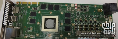
Here is the first true-color picture of the GeForce Kepler 104 (GK104) reference PCB shot in full (well, almost, excluding the uneventful PCIe bus connector). The picture provides a panoramic view of the card's VRM as shown in a drawing posted earlier this day, and reveals the strange double-decker power connector. The card is loaded with a 5-phase NVVDC configuration, as detailed in an older article. It also confirms that the GK104 has a 256-bit wide memory interface, with likely 2 GB standard memory amount. This is also the first picture of the GK104 ASIC, which has square package, and somewhat square die. While the PCB is green in color, it's most likely an engineering sample. The final product (branded GeForce GTX 680 / GTX 670 Ti), could have a black-colored one.
Sources: ChipHell, Expreview
Add your own comment

95 Comments on GK104 PCB Pictured in Full

#51
OneCool
Well theres a picture of it...... meh


W1z needs to be posting a review before I care how many fan connectors it has :laugh::p


WTF is up with the power connectors though.Theres like a freaking stack of them?

I can see to the future a new PSU PCI-E connector spec coming soon
Posted on Reply
#52
Crap Daddy
wolf9/10 of this thread is arguments over a 2 pin connector? come on guys whatabout the KICKASS new GPU on that PCB? the new VRM and pci-e power arrangement, or good old fashioned performance speculation? :)
OK I'll give you a "good old fashion performance speculation".

Kyle Bennet at HardOCP says a few minutes ago:

"I am seeing information out of China this morning showing 45% to 50% performance increase over 580 in canned benchmarks."
Posted on Reply
#54
seronx
alexsubrimeh...
It is a sample board.

ASUS's one is going to be neon red with a black PCB.
I'm joking.
Posted on Reply
#55
badtaylorx
im getting a chubby just thinking of soldering on another 6pin and REALLY seeing what this lil bad bitch can do!!!
Posted on Reply
#56
NorthEndJon
irazerpower connectors is that way, because of big turbine and not enough space for it. - image :)
I think you've nailed it. The power connectors will be stacked because the fan is big.
Posted on Reply
#57
semantics
NorthEndJonI think you've nailed it. The power connectors will be stacked because the fan is big.
maybe but look at the board it looks like it could have 2 pcie female connectors on there but they chose to stack an 6 on an 8 for w.e reason, it's probably an eng sample and nvidia is messing around with ideas. Maybe it will only need a 8 pin and the 6 pin or optional vice versa. But it is nvidia who knows i gave up guessing when they stacked 2 pbcs on top of each other for a dual gpu "solution".
Posted on Reply
#58
OneCool
Isnt this a 22nm part and shouldnt it be better on power consumption?

So whats up with the massive VRM and crazy pci-e power connectors?

5800 Ultra all over again?

The new and improved "dustbuster"
Posted on Reply
#59
NC37
Ahh nekkid PCB photos, the nerd's nudie mag..."Shake it Keppy, you know what we like!" :D
Posted on Reply
#60
newtekie1
Semi-Retired Folder
seronxIt's a 6-pin on top of an 8-pin.
It seems like it depends on which ES you look at. The one from ChipHell seems to be an 8-pin on top of a 6-pin, but the other thread shows just a 6-pin on top of a 6-pin. So it seems like either or depending on the sample. I'm guessing the early samples used 6-pin+8pin because they wanted to make sure they had enough power, and the later samples were reduced to a 6-pin+6-pin once they were sure that is all it needed.
Ferrum MasterI thought we were talking about a connector like in the right bottom corner... that is truly a led connector for 280ties... :laugh:


www.techpowerup.com/reviews/Zotac/GeForce_GTX_280_Amp_Edition/images/front.jpg
Oh yeah, I never even noticed the spot on the GTX280 PCB for the LED connector in the bottom right, probably because it doesn't have the connector actually there. Good eyes! The one at the top next to the power was definitely for the audio pass through like you and I said. So I'm positive the connector on the GK104 PCB is definitely for an LED and not an audio passthrough. Because even if they did need an audio passthrough, nVidia would do what they did with the GT220/240 and just pass it via the PCI-E bus.
Posted on Reply
#61
Benetanegia
Crap DaddyOK I'll give you a "good old fashion performance speculation".

Kyle Bennet at HardOCP says a few minutes ago:

"I am seeing information out of China this morning showing 45% to 50% performance increase over 580 in canned benchmarks."
If that ends up being true (paint me an skeptical face), it will be fun the day reviews come in, everybody could tell me "see? you were wrong, it's not 25% faster than GTX580, it's 50% faster." :laugh:
Posted on Reply
#63
Crap Daddy
BenetanegiaIf that ends up being true (paint me an skeptical face), it will be fun the day reviews come in, everybody could tell me "see? you were wrong, it's not 25% faster than GTX580, it's 50% faster." :laugh:
Here's more cryptic info from the aforementioned Kyle:

"Quote:
Originally Posted by pelo
Is that chiphell you're referring to? If so I'd be wary...

If it is true then let's hope the price wars continue

No, I am not referring to web based resources at all. I never make comments on here based on anything I read online.

Quote:
Originally Posted by boxleitnerb
We're still talking about GK104, right? Canned in what way? Have they solved the high res problem (Fermi didn't do too well there)?

680 vs 580 - Artificial 3D benchmarks."

He says GTX680. Hmmm...
Posted on Reply
#64
semantics
OneCoolIsnt this a 22nm part and shouldnt it be better on power consumption?

So whats up with the massive VRM and crazy pci-e power connectors?

5800 Ultra all over again?

The new and improved "dustbuster"
If newer generations used less power then before then we still be talking about 350w psu vs 300w psu, which was just a hand full of years ago XD, we probably also have more free expansions slots because dual slot monstrosity wouldn't have come out.
Posted on Reply
#65
newtekie1
Semi-Retired Folder
OneCoolIsnt this a 22nm part and shouldnt it be better on power consumption?

So whats up with the massive VRM and crazy pci-e power connectors?

5800 Ultra all over again?

The new and improved "dustbuster"
A 5 phase VRM is massive? You realize the 7970, the part nVidia claims the GK104 will outperform, uses a 5 phase VRM as well, right?

Lowering the nm does yield better power consumption, however if you pair that with also increasing the performance, then the power consumption stays right about the same.
Posted on Reply
#66
MxPhenom 216
ASIC Engineer
NorthEndJonTheres only one 4 pin PWM fan port at the end of the board. The 2 pin at the top has a JP under it, designating it as some sort of jumper. Likely not a fan port. Sorry.
Thats exactly what I was going to say
Posted on Reply
#67
xenocide
newtekie1A 5 phase VRM is massive? You realize the 7970, the part nVidia claims the GK104 will outperform, uses a 5 phase VRM as well, right?

Lowering the nm does yield better power consumption, however if you pair that with also increasing the performance, then the power consumption stays right about the same.
People tend to forget this a lot. Lowering from 40nm to 22nm means you can get the same performance with lower power consumption, but when you try to increase the performance as well, it tends to be about the same. If this card does use the same amount of power as the 7970 and outperforms it... oh damn...
Posted on Reply
#68
bear jesus
The location of the VRMs makes me wonder what the water blocks will look like and if any will have water run over the VRMs, i do not mind the stacked outputs as long as it supports 3 screens from a single card (i am assuming that is the reason for the stacked DVI ports).

Other than that I look forward to the reviews and hope it could be a suitable option for me.
Posted on Reply
#69
newtekie1
Semi-Retired Folder
bear jesusThe location of the VRMs makes me wonder what the water blocks will look like and if any will have water run over the VRMs, i do not mind the stacked outputs as long as it supports 3 screens from a single card (i am assuming that is the reason for the stacked DVI ports).

Other than that I look forward to the reviews and hope it could be a suitable option for me.
It isn't like the manufacturers have to use the stacked DVI and power connectors either. There is a location for a 6-pin next to the stacked power connectors that can be used to make a single slot card, and I'm sure they can drop off a DVI connector if they wanted to, or easily change the output configuration any way they choose just by making very simple changed to the PCB. Look at some of the Zotac cards at launch of the GTX500 series, they had almost completely reference PCBs, but had stacked DVI connectors to add output functionality. Changing the output configuration is probably the easiest PCB change a manufacturer can make.

Also, who is to even say these will support quad-SLI, the previous generation mid-range only did dual-SLI, so these can do triple but maybe not quad, quad might be reserved for the real big boys of this generation which we haven't seen yet.
Posted on Reply
#70
bear jesus
newtekie1It isn't like the manufacturers have to use the stacked DVI and power connectors either. There is a location for a 6-pin next to the stacked power connectors that can be used to make a single slot card, and I'm sure they can drop off a DVI connector if they wanted to, or easily change the output configuration any way they choose just by making very simple changed to the PCB. Look at some of the Zotac cards at launch of the GTX500 series, they had almost completely reference PCBs, but had stacked DVI connectors to add output functionality. Changing the output configuration is probably the easiest PCB change a manufacturer can make.

Also, who is to even say these will support quad-SLI, the previous generation mid-range only did dual-SLI, so these can do triple but maybe not quad, quad might be reserved for the real big boys of this generation which we haven't seen yet.
True but i have 3 DVI screens so i like the 2 DVI ports :p and I only want a single card so being dual slot still when a water block is installed would be a non issue to me.

The previous gen mid range had single SLI bridges i thought? thus they were hardware limited to 2 cards but with 2 bridges the 4 card setup is mainly limited by software support i thought? and if the GK104 is to be named the 680 and 670 surly it is not the mid range and the big boy would be the 690 as in dual GK104?

Honestly i know too little solid info for me to have any idea what is going on with the 6xx generation. :laugh:
Posted on Reply
#71
newtekie1
Semi-Retired Folder
bear jesusTrue but i have 3 DVI screens so i like the 2 DVI ports :p and I only want a single card so being dual slot still when a water block is installed would be a non issue to me.
As I said, the stacked DVIs can be changed to the traditional layout that the GTX500/400 series used without much effort by the manufacturers.
bear jesusThe previous gen mid range had single SLI bridges i thought? thus they were hardware limited to 2 cards but with 2 bridges the 4 card setup is mainly limited by software support i thought?
Yes, the GTX560/460 both had a single SLI connector. But they were always software limitted. The dual-GTX460/560 cards that eVGA put out had another SLI connector on them because hardware wise they could do triple-SLI, but nVidia limitted them via the driver. I wouldn't be surprised if they did the same with the GK104, except they software limit it to triple-SLI.

The GTX285 was supposed to be triple-SLI, but turned out to be software limited too, eVGA's classified card proved that. In fact, G92 was quad-SLI capable too, and the 9800GTX had the two connectors, but the 9800GTX was limited to tri-SLI. To get quad-SLI with G92 you had to use two 9800GX2s. So I wouldn't put it past nVidia to only allow tri-SLI on the GK104, and really I don't see a lot of people buying these for more anyway. I don't see a lot of people buying any card for quad-SLI actually, even the current generation, there are a few but not many.
bear jesusand if the GK104 is to be named the 680 and 670 surly it is not the mid range and the big boy would be the 690 as in dual GK104?

Honestly i know too little solid info for me to have any idea what is going on with the 6xx generation. :laugh:
It is the mid-range. We haven't heard a lot about the high end, but there will be a single GPU that is higher than the GK104, we already know that.
Posted on Reply
#72
bear jesus
newtekie1As I said, the stacked DVIs can be changed to the traditional layout that the GTX500/400 series used without much effort by the manufacturers.
I'm sorry i should have been more clear, i like the 2 stacked DVI ports, i mean it as in i would be happy with the reference model.
newtekie1Yes, the GTX560/460 both had a single SLI connector. But they were always software limitted. The dual-GTX460/560 cards that eVGA put out had another SLI connector on them because hardware wise they could do triple-SLI, but nVidia limitted them via the driver. I wouldn't be surprised if they did the same with the GK104, except they software limit it to triple-SLI.

The GTX285 was supposed to be triple-SLI, but turned out to be software limited too, eVGA's classified card proved that. In fact, G92 was quad-SLI capable too, and the 9800GTX had the two connectors, but the 9800GTX was limited to tri-SLI. To get quad-SLI with G92 you had to use two 9800GX2s. So I wouldn't put it past nVidia to only allow tri-SLI on the GK104, and really I don't see a lot of people buying these for more anyway. I don't see a lot of people buying any card for quad-SLI actually, even the current generation, there are a few but not many.
I just assumed the single bridge could have been a physical limit even if there was no software limit but i agree lots of Nvidia SLI setups are software limited to 3 even when there is no possible hardware limit and it would not be surprising if these are but i have no idea until it is released.
newtekie1It is the mid-range. We haven't heard a lot about the high end, but there will be a single GPU that is higher than the GK104, we already know that.
First i just have to point out according to that link GK104 has a 384-bit bus but it looks like it actually has a 256 bit bus and it also says 640 to 768 CUDA cores but it is now rumored that GK104 has 1536 CUDA cores so really until the NDA is lifted i would not truly trust any information but i should have included a link with my last post which would have explained my last sentence sohere it is now

My main thought is why is GK104 rumored to be the 680 and 670? is it just bad information or is Nvidia changing the naming or is there something else going on?
I truly have no idea until i can see something official as i have read way too many random rumors which are quite possibly untrue.
Posted on Reply
#73
GC_PaNzerFIN
VRM for memory looks same as GTX 570/580. VRM for gpu seems to be upscaled GTX 470 VRM (+1 phase).

Definately built with overclocking in mind otherwise you'd have gone cheaper way. Oh and definately closer to +400€ card, mark my words.
Posted on Reply
#74
newtekie1
Semi-Retired Folder
GC_PaNzerFINVRM for memory looks same as GTX 570/580. VRM for gpu seems to be upscaled GTX 470 VRM (+1 phase).

Definately built with overclocking in mind otherwise you'd have gone cheaper way. Oh and definately closer to +400€ card, mark my words.
Of course it is going to be an expensive card, it is supposed to outperform the HD7970, so it will likely be priced the same or higher.
Posted on Reply
Add your own comment
Nov 21st, 2024 04:33 EST change timezone

New Forum Posts

Popular Reviews

Controversial News Posts