Friday, March 2nd 2012

GK104 PCB Pictured in Full
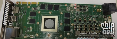
Here is the first true-color picture of the GeForce Kepler 104 (GK104) reference PCB shot in full (well, almost, excluding the uneventful PCIe bus connector). The picture provides a panoramic view of the card's VRM as shown in a drawing posted earlier this day, and reveals the strange double-decker power connector. The card is loaded with a 5-phase NVVDC configuration, as detailed in an older article. It also confirms that the GK104 has a 256-bit wide memory interface, with likely 2 GB standard memory amount. This is also the first picture of the GK104 ASIC, which has square package, and somewhat square die. While the PCB is green in color, it's most likely an engineering sample. The final product (branded GeForce GTX 680 / GTX 670 Ti), could have a black-colored one.
Sources:
ChipHell, Expreview

95 Comments on GK104 PCB Pictured in Full
bcs i really hope that and that the price would be right so i can get EVGA's version ^^
It's 5+1+1, and not 3+1+1 as detailed in the older article.
bcs making a ref design smaller it will fit in more cases so u can make a micro-atx or micro-itx gaming system without need to have a larger case ^^
but hopefully a little lower than that to beat AMD a little ^^
GK104 is only a GeForce part.
GK112 is the new flagship for the Tesla/Quadro series.
GK112 is only a Workstation part.
GK106 once it comes out will take place of the mobile GPUs in the 700 series not the 600 series.
GK107
GK117
GK100
GK110
GF1xx 28 nm
are all dead.
GTX 680 -> 64x8
GTX 670 -> 64x7
GTX 660 -> 64x6
GTX 650 -> 64x5
GTX 645 -> 64x4
with the lower parts just being rebrands till the 700 series
I really would like to see the source that says otherwise.