Tuesday, March 13th 2012

GeForce GTX 680 Specifications Sheet Leaked

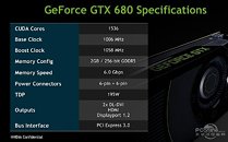
Chinese media site PCOnline.com.cn released what it claims to be an except from the press-deck of NVIDIA's GeForce GTX 680 launch, reportedly scheduled for March 22. The specs sheet is in tune with a lot of information that we already came across on the internet, when preparing our older reports. To begin with the GeForce GTX 680 features clock speeds of 1006 MHz (base), and 1058 MHz (boost). The memory is clocked at a stellar 6.00 GHz (1500 MHz actual), with a memory bus width of 256-bit, it should churn out memory bandwidth of 192 GB/s. 2 GB is the standard memory amount.

For the umpteenth time, this GPU does feature 1,536 CUDA cores. The card draws power from two 6-pin PCIe power connectors. The GPU's TDP is rated at 195W. Display outputs include two DVI, and one each of HDMI and DisplayPort. Like with the new-generation GPUs from AMD, it supports PCI-Express 3.0 x16 bus interface, which could particularly benefit Ivy Bridge and Sandy Bridge-E systems, in cases where the link width is reduced to PCI-Express 3.0 x8 when there are multiple graphics cards installed.
Source: PCOnline.com.cn
Add your own comment

44 Comments on GeForce GTX 680 Specifications Sheet Leaked

#26
Benetanegia
ImsochoboIbm shows that it's possible, but I agree with you, but there are other ways to design stuff that goes around that problem you state, but Nvidia is doing the right thing.
There are ways to circumvent and alleviate that problem a little bit, but in most cases it requires doing it "by hand" which is fine for CPUs and long design cycles, but it's rare in GPU world, where most of the design is automated. I've never heard of hand crafted GPUs tbh.

Which may actually be the case with Kepler to an extent. Cadaveca suggested it somewhere and it may very well be true for Kepler after all. According to all the data we can collect Nvidia's shaders have not changed much since G80, apart from adding functionality, expanding the ISA, etc, but on the most basic level they're almost the same. For a company like Nvidia, wanting to enter HPC so badly it may make a lot of sense to take their single most important, yet small, element and completely hand craft it. Considerig it's going to be used for several years and when packed together in the thousands, they take up 60-70% of die size easily, it does make sense.

And there were rumors about Nvidia changing the SPs for project Echelon (I think that was the name for the DARPA funded project) and that it would posibly make it into Maxwell. But release dates have been pushed back by 28 nm, so maybe some of the changes made it into Kepler?
Posted on Reply
#28
cadaveca
My name is Dave
BenetanegiaAnd there were rumors about Nvidia changing the SPs for project Echelon (I think that was the name for the DARPA funded project) and that it would posibly make it into Maxwell. But release dates have been pushed back by 28 nm, so maybe some of the changes made it into Kepler?
I look at it this way:

Any company, no matter the industry, will always cater to their largest customer, and then adapt what they can to meet the needs of other smaller customers...but that big customer is always priority #1.


So, who is nVidia's largest paying customer? Answer that question, and I think any questions about potential changes in architectural design will be answered, as well as targeted performance for said designs.


Of course, you do have to figure in issues like sourcing components and such...
Posted on Reply
#29
TheoneandonlyMrK
btarunrthis GPU does feature 1,536 CUDA cores
im thinking now, from going off previouse rumours of a split shader architecture(with some assigned solely GFX workloads) ,we may be in for some thing were not expecting ,as to me all the reports are over stateing the CUDA 1,536 cores , could NV have thrown additional special gfx use shaders in their as well ;) not countable as CUDA cores ,they did say expect to be blown away and for something different

seems such a soddin odd number too
Posted on Reply
#30
Crap Daddy
theoneandonlymrkseems such a soddin odd number too
It's not. Four times CUDA cores of the GF114.
Posted on Reply
#31
MxPhenom 216
ASIC Engineer
Crap DaddyIt's not. Four times CUDA cores of the GF114.
yet that won't mean 4 times the performance either, since the Cores are significantly weaker then those of Fermi cores.

according to the recent spec slide ti appears Kepler is going to have insanely fast memory. 6ghz clock!
Posted on Reply
#32
Crap Daddy
nvidiaintelftwaccording to the recent spec slide ti appears Kepler is going to have insanely fast memory. 6ghz clock!
Yep, another surprise. If it's true then a spectacular way to mend the memory controller and beat AMD at its own game.
Posted on Reply
#33
Benetanegia
cadavecaI look at it this way:

Any company, no matter the industry, will always cater to their largest customer, and then adapt what they can to meet the needs of other smaller customers...but that big customer is always priority #1.


So, who is nVidia's largest paying customer? Answer that question, and I think any questions about potential changes in architectural design will be answered, as well as targeted performance for said designs.


Of course, you do have to figure in issues like sourcing components and such...
I don't know who is their largest customer now, a little help would be appreciated instead of the mistery. Consumer GPU revenues have been declining, professional market has been growing, is that what you mean? The last time I saw a breakdown, by revenue consumer GPU was usually 2x as big as professional market, by gross margin it was the opposite, while profits were more or less the same. I don't know how it stands now.

In any case I don't see it as relevant. A more efficient shader architecture is good for both HPC and GPUs so IMO its irrelevat which target customer fueled the change. That they were changing the shaders for Maxwell is pretty much a fact. It was not expected for Kepler, but maybe...
Posted on Reply
#34
Vulpesveritas
BenetanegiaI don't know who is their largest customer now, a little help would be appreciated instead of the mistery. Consumer GPU revenues have been declining, professional market has been growing, is that what you mean? The last time I saw a breakdown, by revenue consumer GPU was usually 2x as big as professional market, by gross margin it was the opposite, while profits were more or less the same. I don't know how it stands now.

In any case I don't see it as relevant. A more efficient shader architecture is good for both HPC and GPUs so IMO its irrelevat which target customer fueled the change. That they were changing the shaders for Maxwell is pretty much a fact. It was not expected for Kepler, but maybe...
Nvidia's largest customers right now are at the enterprise and smartphone levels.
And it's funny you mention marketshare of GPUs, seeing as AMD has nearly a 10% lead on Nvidia in the GPU marketshare department right now.
Posted on Reply
#35
Benetanegia
VulpesveritasAnd it's funny you mention marketshare of GPUs, seeing as AMD has nearly a 10% lead on Nvidia in the GPU marketshare department right now.
Yes and no. Those figures include APUs and other kinds of integrated GPU. It only reflects the fact that Nvidia no longer sells integrated GPUs and the fact that every Intel CPU and most (by sales) AMD CPUs are sold with an integrated GPU. So unless you pretend now that Intel is the largest (almost 3x bigger than AMD) graphics card manufacturer, your point is moot. When it comes to discrete GPUs Nvidia's share is almost twice as much as AMD's. I don't know why you bring this into this thread, instead the other one.

As for what is their biggest customer, smartphone companies, definitely are not. Enterprise, by revenue, it's not, I don't think so. If it IS, provide proof please.
Posted on Reply
#36
Vulpesveritas
BenetanegiaYes and no. Those figures include APUs and other kinds of integrated GPU. It only reflects the fact that Nvidia no longer sells integrated GPUs and the fact that every Intel CPU and most (by sales) AMD CPUs are sold with an integrated GPU. So unless you pretend now that Intel is the largest (almost 3x bigger than AMD) graphics card manufacturer, your point is moot. When it comes to discrete GPUs Nvidia's share is almost twice as much as AMD's. I don't know why you bring this into this thread, instead the other one.

As for what is their biggest customer, smartphone companies, definitely are not. Enterprise, by revenue, it's not, I don't think so. If it IS, provide proof please.
I had remembered reading that, however I am unable to find a link to the numbers unfortunately. I will fully concede you that.
Posted on Reply
#37
hhumas
awesome .. that is why I wait and didn't go for ATi
Posted on Reply
#38
OneCool
Wrigleyvillainlol same comment gen after gen after gen.
Its like clock work every time. :rolleyes: EVERY FREAKING TIME!!!!!!!!!!!!!

AMD/Ati releases their best stuff blindly I may add and nVidia holds out to make sure they can beat it,whether it takes 2 to 4 months from AMD/Ati's release.

rinse and repeat :D

NVIDIA - "THE WAY CHICKEN SHIT IS MEANT TO BE PLAYED"
Posted on Reply
#39
DarkOCean
OneCoolIts like clock work every time. :rolleyes: EVERY FREAKING TIME!!!!!!!!!!!!!

AMD/Ati releases their best stuff blindly I may add and nVidia holds out to make sure they can beat it,whether it takes 2 to 4 months from AMD/Ati's release.

rinse and repeat :D

NVIDIA - "THE WAY CHICKEN SHIT IS MEANT TO BE PLAYED"
This is how a duopoly works.
Posted on Reply
#40
Zerono
I still dont get why it has a 256bit memory bus shouldn't it be higher?
Posted on Reply
#41
xenocide
ZeronoI still dont get why it has a 256bit memory bus shouldn't it be higher?
The GK104 was originally intended to be midrange, so they designed it accordingly, hence no 384-bit or higher memory bus. I assume they decided they didn't need it.
Posted on Reply
#42
Steevo
Imsochobomhz and die size have nothing in common....
BenetanegiaYes it does. If you want an electronic device to clock higher you have to shorten the path between input and output and that means going parallel with (duplicating at transistor level) a lot of things that would otherwise be serial and means you have to invest much more transistors on it. That takes up much more space and transistors and that also means more complicated control & logic, which once again means more transistors. Which once again means more active transistors for the same job, which means higher TDP, which means higher temps, which actually means higher TDP, which actually means lower posible clocks, which actually means you have to invest even more transistors in order to achieve a certain clock, which means higher TDP and the process keeps going on and on and on.
This is true.^


Decoupling capacitors on die and termination of a high drive strength signal means more drains, and more power to run the circuits at the higher speed.
Posted on Reply
#44
jpierce55
cadavecaThat'd be awesome, as I generally have a good understanding of hardware, but this stuff blows my mind.:laugh:


Funny how it needs to be repeated. Personally, because i don't get what's going on with these card, I reserve all judgement until after I get to read W1zz's review, which i guess is incoming at some point.


I'm still laughing at the fact that the "chocolate" was in fact a cookie. That mis-conception alone, based on appearances, says quite a bit.
Nvidia will never try to take out AMD and AMD will never try to take out Nvidia. If the other company failed it would hurt them, because they would likely get split due to the monopoly. We might see times when 1 card is remarkably faster than the other companies card, but I doubt we will ever see a grand slam.
Posted on Reply
Add your own comment
Dec 23rd, 2024 14:18 EST change timezone

New Forum Posts

Popular Reviews

Controversial News Posts